My Menu
8 Pin DIP IC Socket Base Adaptor

8 Pin DIP IC Socket Base Adaptor

(0)
8 Pin IC Base An 8-pin IC base refers to a type of integrated circuit (IC) package that has 8 pins or leads for connecting the IC to a circuit board. These pins are typically arranged in a dual in-line package (DIP) configuration, with two rows of four pins each. 8-pin ICs are often small and simple ICs that are widely used in many electronic devices and appliances, such as timers, oscillators, and digital logic circuits, for example, 555 timer IC , LM358 IC, etc. The 8-pin DIP package is one of the most common IC package formats, and it …
Condition: NEW
As low as ₹3.26   ₹22.40 Incl. GST (No Hidden Charges)
Backorder Available Delivery: Next Day Delivery
IN STOCK SKU#: IOT-2418
Delivery & Pickup Options
Get it Next Day on Order

Order now and we'll have it ready for delivery by the next business day.

For bulk orders or wholesale inquiries, please contact us at Email: support@iotcart.in or call/message us at Phone: 8050206487.

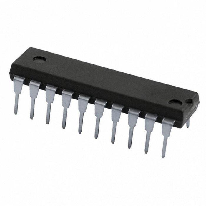
8 Pin IC Base An 8-pin IC base refers to a type of integrated circuit (IC) package that has 8 pins or leads for connecting the IC to a circuit board. These pins are typically arranged in a dual in-line package (DIP) configuration, with two rows of four pins each. 8-pin ICs are often small and simple ICs that are widely used in many electronic devices and appliances, such as timers, oscillators, and digital logic circuits, for example, 555 timer IC , LM358 IC, etc. The 8-pin DIP package is one of the most common IC package formats, and it is often used for ICs that have a small number of input and output pins. This package is relatively easy to work with, as the pins are widely spaced and can be easily inserted into a breadboard or soldered onto a circuit board. This is 8 Pin IC Base with a pin-to-pin spacing of 2.54mm and a width of 7.62mm (300 mil). Features: 8 Pin DIP IC Socket Base Adaptor Molded notch for proper orientation Easy to insert and remove ICs Compatible with 8-pin ICs in dual in-line package (DIP) configuration Reliable and durable design Applications: Circuit prototyping: Facilitates easy testing and swapping of 8-pin ICs during circuit development. Electronic projects: Useful for hobbyists and DIY enthusiasts working on projects involving timers, oscillators, and digital logic circuits. Breadboarding: Compatible with breadboards, making it convenient for temporary circuit setups and experimentation. Embedded systems development: Useful in the prototyping phase of embedded systems where different ICs may need testing. Robotics projects: Can be incorporated into robotics projects that involve 8-pin ICs for control and processing. Automation projects: Suitable for applications requiring small-scale automation using 8-pin ICs.

  • 8-pin DIP socket with 2.54mm pin spacing
  • Molded notch for correct IC orientation
  • Compatible with NE555, LM358, CD4011, and 74-series ICs
  • Reusable design for prototyping and testing
  • Suitable for breadboards and perfboards
  • Prevents IC damage during soldering
  • Ensures reliable electrical contact
  • Easy IC insertion and removal
  • Notch for polarity protection
  • Ideal for prototyping and development
Pin spacing 0.1 inches (2.54 mm)
Pin 18
Dimension 10x10x4mm
Weight 2g
What ICs are compatible with this 8-pin DIP socket?

Compatible with all standard 8-pin DIP ICs including NE555, LM358, CD4011, and 74-series logic chips.

Can this IC socket be used on a breadboard?

Yes, the 2.54mm pin spacing allows direct insertion into breadboards and perfboards.

How does the molded notch help?

The notch ensures correct IC orientation, preventing reverse insertion and circuit damage.

Is this socket reusable?

Yes, designed for repeated IC insertion and removal without degradation.

To rate this product please login!

About 8 Pin DIP IC Socket Base Adaptor by Iotcart

Shop 8 Pin DIP IC Socket with 2.54mm spacing. Compatible with NE555, LM358, CD4011. Ideal for breadboarding & prototyping. Buy now in India.

Categorised under: Integrated Circuits

Related products

Related products

Buy 74HC85 4-bit Magnitude Co…
(0)
4-bit Magnitude Comparator IC - 74HC85 The 74HC Series 74HC85 are high-speed Si-gate CMOS devices and are pin-compatible with low-power Schottky TTL (LSTTL). They are specified in compliance with JEDEC standard no. 7A. The 74HC85 IC are 4-bit magnitude comparators that can be expanded to almost any length. They perform the comparison of two 4-bit binary, BCD, or other monotonic codes and present the three possible magnitude results at the outputs (QA>B, QA=B and QAB, IA=B and IAB = = LOW and IA=B = HIGH. For words greater than 4-bits, units can be cascaded by connecting outputs QA? and QA=B to the corresponding inputs of the significant comparator. Pinout: Pinout of 74HC85 IC
₹23.84  
Backorder Available
₹47.60
Incl. GST (No Hidden Charges)
Buy 74HC02 Quad 2-Input NOR G…
(0)
74HC02 - Quad 2-Input NOR Gate IC The 74HC Series 74HC02 IC is a 14-Pin Quad 2-Input NOR Gate IC. NOR gates utilize advanced silicon-gate CMOS technology to achieve operating speeds similar to LS-TTL gates with the low power consumption of standard CMOS integrated circuits. All gates have buffered outputs, providing high noise immunity and the ability to drive 10 LS-TTL loads. The 74HC logic family is functionally as well as pin-out compatible with the standard 74LS logic family. All inputs are protected from damage due to static discharge by internal diode clamps to VCC and the ground. Pinout: Pinout Of 74HC02 IC Also check 74LS12 NAND Gate IC (Pack of 5) . Which is used for logical decision making and circuits involving conditional operations.
₹17.33  
Backorder Available
₹40.60
Incl. GST (No Hidden Charges)
Buy CD4009 CMOS Hex Buffer/Co…
(0)
CMOS Hex Buffers/Converter IC - CD4009 CD4009 Hex Buffer/Converters may be used as CMOS to TTL or DTL logic-level converters or CMOS high-sink-current drivers. The CD4009 types are supplied in 16-lead hermetic dual-in-line ceramic packages (F3A suffix), 16-lead dual-in-line plastic packages (E suffix). check out : CMOS 8-Input NAND/AND Gate IC - CD4068 Applications: CMOS to DTL/TTL hex converter CMOS current "sink" or "source" driver CMOS high-to-low logic-level converter Multiplexer — 1 to 6 or 6 to 1 check out : Hex Buffer/Converter IC - CD4010
₹29.26  
Backorder Available
₹47.60
Incl. GST (No Hidden Charges)
Iotcart CD4068 CMOS 8-Input N…
(0)
CMOS 8-Input NAND/AND Gate IC - CD4068 The CD4068 CMOS 8-Input NAND/AND gate IC (Integrated Circuits) provides the system designer with direct implementation of the positive logic 8-Input NAND and AND functions and supplements the existing family of CMOS gates. The CD4x Series CD4068 is an 8-Input NAND/AND Gate CMOS logic-based IC belonging to a CD4000 series of integrated circuits. Firstly, Two output options are available such as AND and NAND gate. Secondly, the same input pins deliver both logical functions. It is available in a variety of packages which includes 14-pin PDIP, GDIP, PDSO. The typical operating voltage of the IC is +5V, but it can also be operated +10V and +15V. It has a standard symmetric output. This IC is useful for applications requiring low power. Furthermore, it offers a wide voltage operating range. check out : CMOS Hex Buffers/Converter IC - CD4009 Pinout: Pinout of CD4068
₹27.09  
Backorder Available
₹54.60
Incl. GST (No Hidden Charges)
Iotcart CD4067 16-Channel Ana…
(0)
16-Channel Analog Multiplexer/Demultiplexer IC - CD4067 CD4067 CMOS analog multiplexers/demultiplexers are digitally controlled analog switches having low ON impedance, low OFF leakage current, and internal address decoding. In addition, the ON resistance is relatively constant over the full input-signal range. The CD4067 is a 16-channel multiplexer with four binary control inputs, A, B, C, D, and an inhibit input, arranged so that any combination of the inputs selects one switch. A logic “1” present at the inhibit input turns all channels off. The CD4067 type are supplied in 24-lead hermetic dual-in-line ceramic packages (F3A suffix), 24-lead dual-in-line plastic packages (E suffix), 24-lead small-outline packages (M, M96, and NSR suffixes), and 24-lead thin shrink small-outline packages (P and PWR suffixes). check out : CD4066 - Quad Bilateral Switch IC Applications: Analog and digital multiplexing and demultiplexing A/D and D/A conversion Signal gating
₹169.06  
Backorder Available
₹278.60
Incl. GST (No Hidden Charges)
CD4081 Quad 2-Input AND Gate …
(0)
CD4081 - Quad 2 Input AND Gate IC CD4081 Quad 2 Input AND gates IC provides the system designer with direct implementation of the AND function and supplements the existing family of CMOS gates. The CD4081 types are supplied in 14-lead hermetic dual-in-line ceramic packages (F3A suffix), 14-lead dual-in-line plastic packages (E suffix), 14-lead small-outline packages (M, MT, M96, and NSR suffixes), and 14-lead thin shrink small-outline packages (PW and PWR suffixes). check out : CD4532 - 8 Bit Priority Encoder IC (Original) Pinout: Pinout Of CD4081 IC check out : CD4030 - Quad 2-Input Exclusive OR (EXOR) Gate IC
₹18.42  
Backorder Available
₹42.00
Incl. GST (No Hidden Charges)
CD4099 8-Bit Addressable Latc…
(0)
CD4099 - 8 bit Addressable Latch IC The CD4099 8-bit addressable latch IC is a serial-input, parallel-output storage register that can perform a variety of functions. Data are inputted to a particular bit in the latch when that bit is addressed (by means of input A0, A1, A2) and when WRITE DISABLE is at a low level. When WRITE DISABLE is high, data entry is inhibited; however, all 8 outputs can be continuously read independently of WRITE DISABLE and address inputs. A master RESET input is available, which resets all bits to a logic "0" level when RESET and WRITE DISABLE is at a high level. When RESET is at a high level, and WRITE RESET is at a low level, the latch acts as a 1-of-8 demultiplexer; the bit that is addressed has an active output that follows the data input, while all unaddressed bits are held to a logic "0" level. The CD4099 types are supplied in 16-lead hermetic dual-in-line ceramic packages (F3A suffix), 16-lead dual-in-line plastic packages (E suffix), 16-lead small-outline packages (M, M96, MT, and NSR suffixes), and 16-lead thin shrink small-outline packages (PW and PWR suffixes). check out : Quad NOR R-S Latch Tri-state IC - CD4043 Pinout: Pin No Pin Name Description 1 Q7 Output Pin 7 of Latch 2 CL Clear Output Pin 3 D Data Input 4 E’ Enable Pin 5 A0 Input Pin 0 of Latch 6 A1 Input Pin 1 of Latch 7 A2 Input Pin 2 of Latch 8 VSS Source Supply 9 Q0 Output Pin 0 of Latch 10 Q1 Output Pin 1 of Latch 11 Q2 Output Pin 2 of Latch 12 Q3 Output Pin 3 of Latch 13 Q4 Output Pin 4 of Latch 14 Q5 Output Pin 5 of Latch 15 Q6 Output Pin 6 of Latch 16 VDD Drain Supply Applications: Multi-line decoders A/D converters
₹28.18  
Backorder Available
₹49.00
Incl. GST (No Hidden Charges)
CD4514 4-to-16 Line Decoder I…
(0)
CD4514 - 4 Bit Latch/4-16 Line Decoder IC The CD4x Series CD4514 IC is a 4-to-16-line decoder with latched inputs implemented with complementary MOS (CMOS) circuits constructed with N- and P-channel enhancement mode transistors. These circuits are primarily used in decoding applications where low power dissipation and/or high noise immunity are required. The CD4514 (output active high option) presents a logical “1” at the selected output. The input latches are R–S type flip-flops, which hold the last input data presented prior to the strobe transition from “1” to “0”. This input data is decoded and the corresponding output is activated. An output inhibits line is also available. Pinout: Pinout Of CD4514 IC
₹169.06  
Backorder Available
₹278.60
Incl. GST (No Hidden Charges)
74HC4060 14-Stage Binary Coun…
(0)
14-Stage Binary Ripple Counter IC - 74HC4060 The 74HC Series 74HC4060 IC is a high-speed binary ripple-carry counter. These counters are implemented utilizing advanced silicon-gate CMOS technology to achieve speed performance similar to LS-TTL logic while retaining the low power and high noise immunity of CMOS. The 74HC4060 is a 14-stage counter, which the device increments on the falling edge (negative transition) of the input clock, and all their outputs are reset to a low level by applying a logical high on their reset input. The 74HC4060 also has two additional inputs to enable the easy connection of either an RC or crystal oscillator. This device is pin equivalent to the CD4060. All inputs are protected from damage due to static discharge by protection diodes to VCC and the ground. Pinout: Pinout Of 74HC4060 IC
₹29.26  
Backorder Available
₹54.60
Incl. GST (No Hidden Charges)
Iotcart 74HC139 Dual 2-to-4 L…
(0)
Dual 2-to-4 line Decoder/Demultiplexer IC - 74HC139 The 74HC Series 74HC139 comprises two separate two-line-to-four-line decoders in a single package. The active-low enable input can be used as a data line in demultiplexing applications. All of these decoders/demultiplexers feature fully buffered inputs, presenting only one normalized load to its driving circuit. All inputs are clamped with high-performance Schottky diodes to suppress line-ringing and simplify system design. These Schottky-clamped circuits are designed to be used in high-performance memory-decoding or data-routing applications, requiring very short propagation delay times. In high-performance memory systems, these decoders can be used to minimize the effects of system decoding. When used with high-speed memories, the delay times of these decoders are usually less than the typical access time of the memory. This means that the effective system delay introduced by the decoder is negligible. Pinout: Pinout Of 74HC139 IC Symbol Pin Description 1E, 2E 1, 15 enable input (active LOW) 1A0, 1A1 2, 3 address input 1Y0, 1Y1, 1Y2, 1Y3 4, 5, 6, 7 output (active LOW) GND 8 ground (0 V) 2Y0, 2Y1, 2Y2, 2Y3 12, 11, 10, 9 output (active LOW) 2A0, 2A1 14, 13 address input VCC 16 positive supply voltage Also check 4 Bit D-Latch 74LS75 IC . It's a small, 16-pin integrated circuit (IC) chip that stores 4 bits of digital data. It's commonly used in digital circuits for data storage, timing control, and logic functions.
₹32.51  
Backorder Available
₹61.60
Incl. GST (No Hidden Charges)
Iotcart 74HC541 Octal 3-State…
(0)
Octal 3-State Buffer/Line Driver IC - 74HC541 The 74HC Series 74HC541 IC is an octal non-inverting buffer/line driver with 3-state outputs. The device features two output enables (OE1 and OE2). A HIGH on OEn causes the outputs to assume a high-impedance OFF-state. Inputs include clamp diodes that enable the use of current limiting resistors to interface inputs to voltages in excess of VCC. check out : Octal 3-State Buffer/Line Driver IC - 74HC244 Pinout: Pinout of 74HC541 IC Applications: Industrial Automation & Process Control Signal Processing Automotive
₹27.09  
Backorder Available
₹54.60
Incl. GST (No Hidden Charges)
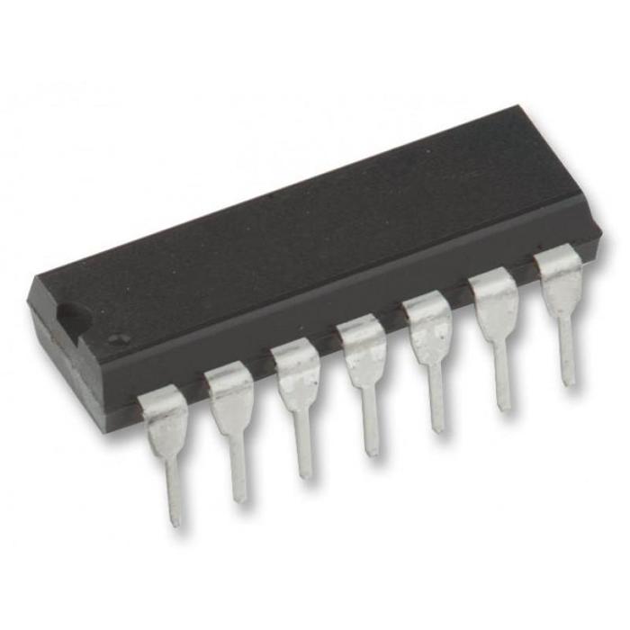
CD4020 14 Stage Binary Counte…
(0)
14 Stage Ripple Carry Binary Counter IC - CD4020 The CD4020 IC is a ripple-carry binary counter. All counter stages are master-slave flip-flops. The state of a counter advances one count on the negative transition of each input pulse; a high level on the RESET line resets the counter to its all-zeros state. Schmitt's trigger action on the input-pulse line permits unlimited rise and fall times. All inputs and outputs are buffered. The CD4x Series CD4020 type is supplied in 16-lead hermetic dual-in-line ceramic packages (F3A suffix), 16-lead dual-in-line plastic packages (E suffix), 16-lead small-outline packages (NSR suffix), and 16-lead thin shrink small-outline packages (PW and PWR suffixes). check out : CD4040 - 12-Stage Ripple Carry Binary Counter IC Pinout: Pinout of CD4020 IC Applications: Control counters Timers Frequency dividers Time-delay circuits
₹20.59  
Backorder Available
₹44.80
Incl. GST (No Hidden Charges)
CD4040 12-Stage Binary Counte…
(0)
CD4040 - 12-Stage Ripple Carry Binary Counter IC The CD4x Series CD4040 is a ripple-carry binary counter that features 12 stages, push-pull type, and balanced outputs, with standard speed (TPD > 50ns). All counter stages are master-slave flip-flops. Supports wide input voltage ranges from 3V to 18V. The maximum input current at 18V is 1 uA whereas 100 nA at 18V and 25°C. All counter stages are master-slave flip-flops. The state of a counter advances one count on the negative transition of each input pulse; a high level on the RESET line resets the counter to its all-zeros state. Schmitt's trigger action on the input-pulse line permits unlimited rise and fall times. All inputs and outputs are buffered. 16 Pin DIP is available in a hermetic dual-in-line ceramic package. We also have a CD4020 with similar features. The differences are CD4020 is a 14 Stage binary counter whereas CD4040 is a 12 Stage binary counter and there is a difference between the pin layout. check out : CD4518 - Dual BCD Up Counter IC (Original) Pinout: Pinout of CD4040 IC Applications: Control Counters Timers Frequency Dividers Time-Delay Circuits
₹30.35  
Backorder Available
₹47.60
Incl. GST (No Hidden Charges)
Buy 74HC11 Triple 3-Input AND…
(0)
74HC11 - Triple 3-Input AND Gate IC The 74HC11 is a digital integrated circuit (IC) with three separate 3-input AND gates. It belongs to the 74HC family of integrated circuits, which are high-speed CMOS (Complementary Metal-Oxide-Semiconductor) devices with quick switching rates and low power consumption. The 74HC Series 74HC11 has three inputs and one output for each AND gate. Only if all of the inputs are high is the output (logic 1) high (logic 1). The output is low if any of the inputs is low (logic 0). (logic 0). As a result, the 74HC11 can be used to create logic functions that require the combination of many signals. The 74HC11 comes in a typical DIP (Dual In-line Package) form factor and is easily incorporated into circuits utilising through-hole technology. It can handle input and output voltages ranging from 0V to Vcc and operates across a wide voltage range of 2V to 6V. Pinout: Pinout Of 74HC11 IC
₹26.01  
Backorder Available
₹50.40
Incl. GST (No Hidden Charges)
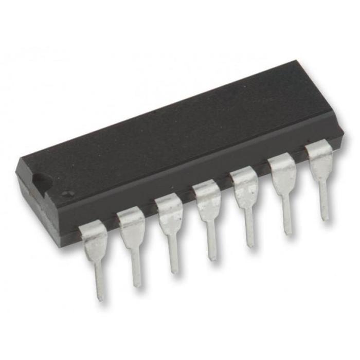
CD4027 Dual JK Flip Flop IC -…
(0)
Dual JK Flip Flop IC - CD4027 CD4027 is a single monolithic chip integrated circuit containing two identical complementary-symmetry J-K master-slave flip-flops. Each flip-flop has provisions for individual J, K, Set, Reset, and Clock input signals. Buffered Q and Q\ signals are provided as outputs. This input-output arrangement provides for compatible operation with the RCA-CD4013B dual D-type flip-flop. The CD4x Series CD4027 is useful in performing control, register, and toggle functions. Logic levels present at the J and K inputs along with internal self-steering control the state of each flip-flop; changes in the flip-flop state are synchronous with the positive-going transition of the clock pulse. Set and reset functions are independent of the clock and are initiated when a high-level signal is present at either the Set or Reset input. The CD4027 types are supplied in 16-lead hermetic dual-in-line ceramic packages (F3A suffix), 16-lead dual-in-line plastic packages (E suffix), 16-lead small-outline packages (M, M96, MT, and NSR suffixes), and 16-lead thin shrink small-outline packages (PW and PWR suffixes). check out : CD4046 - Micropower Phase Locked Loop IC Pinout: Pinout of CD4027 IC
₹28.18  
Backorder Available
₹54.60
Incl. GST (No Hidden Charges)
Features

icon

Full Screen mode

Mode
On
Off

Dark mode

Mode
On
Off

Clear local storage

Clear Cache & Default
0