

Sort by

Browsing
Clock & Timer IC
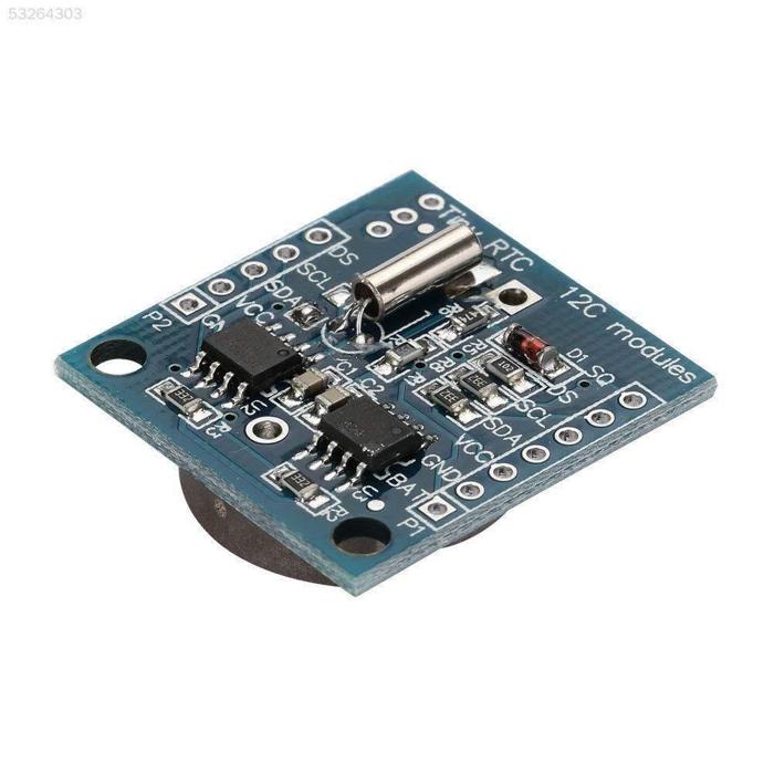
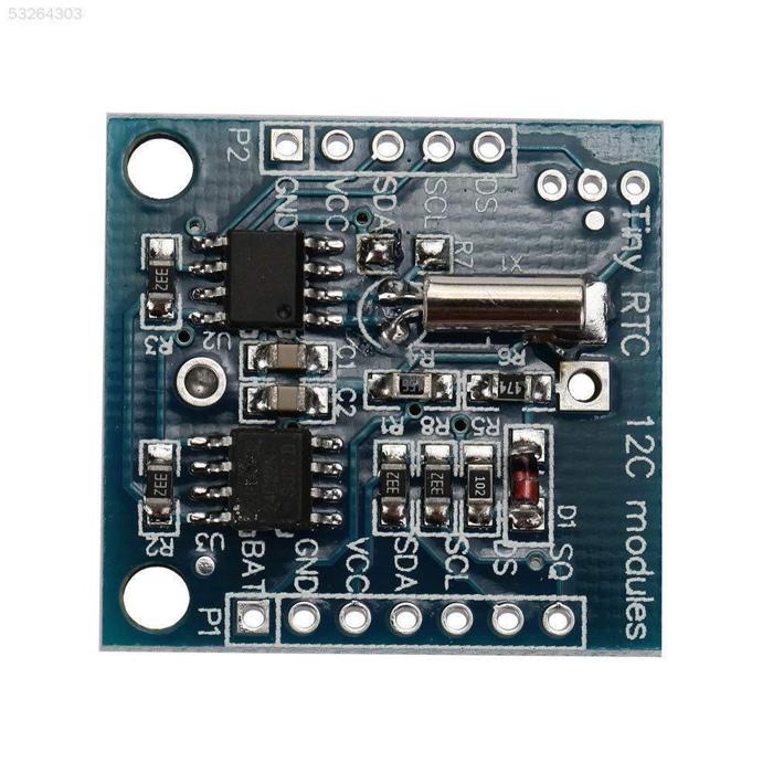
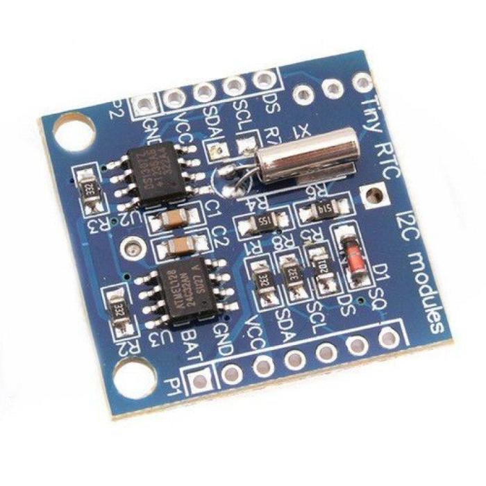
DS1307 Real Time Clock Module
DS1307 Real Time Clock Module
The DS1307 is a low-power clock/calendar with 56 bytes of battery backup SRAM. The clock/calendar provides seconds, minutes, hours, day, date, month and year-qualified data. The end date of each month is automatically adjusted, especially for months with less than 31 days.
This is Tiny RTC Real Time Clock DS1307 I2C IIC Module for
Arduino
. It contains a DS1307
real-time clock IC
. It’s one of the easiest to use RTCs out there, with Arduino and other libraries or simply use I2C commands to set and retrieve the time and date.
Along with the DS1307 real-time clock, the module also has an Atmel 24C32 EEPROM chip which is handy for storing data without worrying about power loss. There is also space on the board to solder your own DS18B20 temperature sensor.
DS1307 Real Time Clock module is used to track the current time and date. It is generally used in computers, laptops, mobiles, embedded system applications devices, etc. In many embedded systems, we need to put timestamps while logging data i.e. sensor values, GPS coordinates, etc. For getting timestamps, we need to use RTC (Real Time Clock). This module is based on the DS1307 IC from Dallas. It uses a 32.768 kHz clock. And supports I2C Interface.
Pinout of DS1307:
Pinout of DS1307 Real Time Clock Module
Pin 1, 2:
Connections for standard 32.768 kHz quartz crystal. The internal oscillator circuitry is intended for operation with a crystal having a specified load capacitance of 12.5pF. X1 is the input to the oscillator and can alternatively be connected to an external 32.768 kHz oscillator. The output of the internal oscillator, X2 is drifted if an external oscillator is connected to X1.
Pin 3
: Battery input for any standard 3V lithium cell or another energy source. Battery voltage should be between 2V and 3.5V for suitable operation. The nominal write-protect trip point voltage at which access to the RTC and user RAM is denied is set by the internal circuitry as 1.25 x VBAT nominal. A lithium battery with 48mAhr or greater will back up the DS1307 for more than 10 years in the absence of power at 25ºC. UL is recognized to ensure against reverse charging current when utilized as part of conjunction with a lithium battery.
Pin 4:
Ground.
Pin 5:
Serial data input/output. The input/output for the I2C serial interface is the SDA, which is the open drain and requires a pull-up resistor, allowing a pull-up voltage of 5.5V. Regardless of the voltage on VCC.
Pin 6:
Serial clock input. It is the I2C interface clock input and is used in data synchronization.
Pin 7:
Square wave/output driver. When enabled, the SQWE bit set to 1, the SQW/OUT pin outputs one of four square-wave frequencies (1Hz, 4 kHz, 8 kHz, and 32 kHz). This is also an open drain and requires an external pull-up resistor. It requires the application of either Vcc or Vb at to operate SQW/OUT, with an allowable pull-up voltage of 5.5V and can be left floating, if not used.
Pin 8:
Primary power supply. When the voltage is applied within normal limits, the device is fully accessible and data can be written and read. When a backup supply is connected to the device and VCC is below VTP, read and write are inhibited. However, at low voltages, the timekeeping function still functions.
₹53.10
Incl. GST (No Hidden Charges)
Backorder Available
₹96.60
Incl. GST (No Hidden Charges)
DS1307 Real Time Clock Module
DS1307 Real Time Clock Module The DS1307 is a low-power clock/calendar with 56 bytes of battery backup SRAM. The clock/calendar provides seconds, minutes, hours, day, date, month and year-qualified data. …
As low as
₹53.10
₹53.10
₹96.60
Incl. GST (No Hidden Charges)
Backorder Available

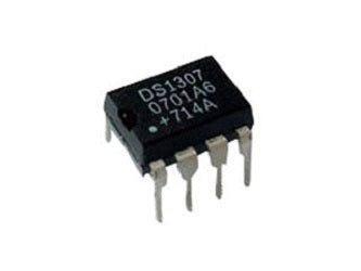
DS1307 RTC IC (Real Time Cloc…
The DS1307 serial real-time clock (RTC) is a lowpower, full binary-coded decimal (BCD) clock/calendar plus 56 bytes of NV SRAM. Address and data are transferred serially through an I2C, bidirectional bus.
The clock/calendar provides seconds, minutes, hours, day, date, month, and year information. The end of the month date is automatically adjusted for months with fewer than 31 days, including corrections for leap year. The clock operates in either the 24-hour or 12- hour format with AM/PM indicator. The DS1307 has a built-in power-sense circuit that detects power failures and automatically switches to the backup supply. Timekeeping operation continues while the part operates from the backup supply.
₹92.11
Incl. GST (No Hidden Charges)
Backorder Available
₹176.40
Incl. GST (No Hidden Charges)
DS1307 RTC IC (Real Time Clock)
The DS1307 serial real-time clock (RTC) is a lowpower, full binary-coded decimal (BCD) clock/calendar plus 56 bytes of NV SRAM. Address and data are transferred serially through an I2C, bidirectional …
As low as
₹92.11
₹92.11
₹176.40
Incl. GST (No Hidden Charges)
Backorder Available
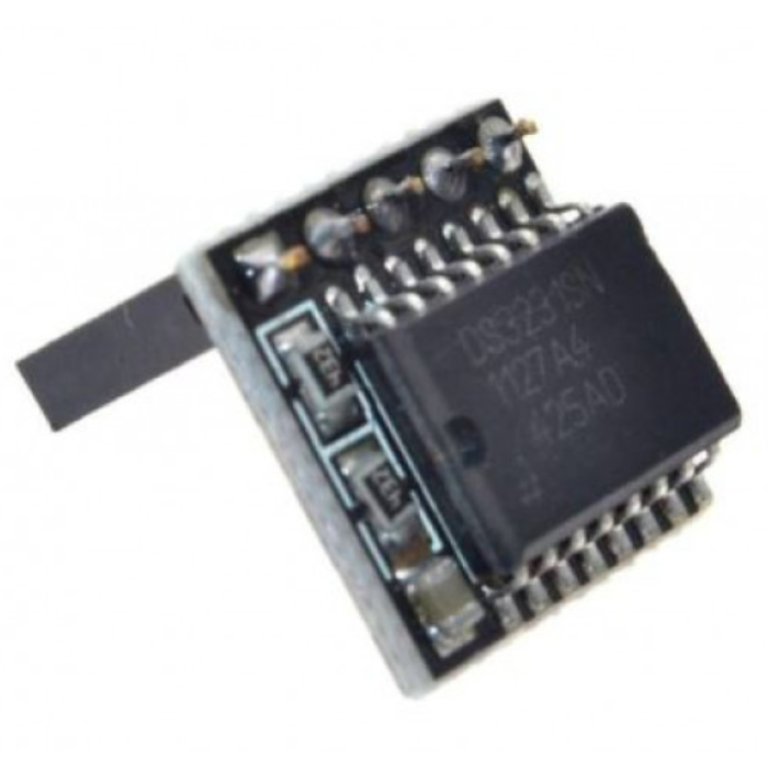
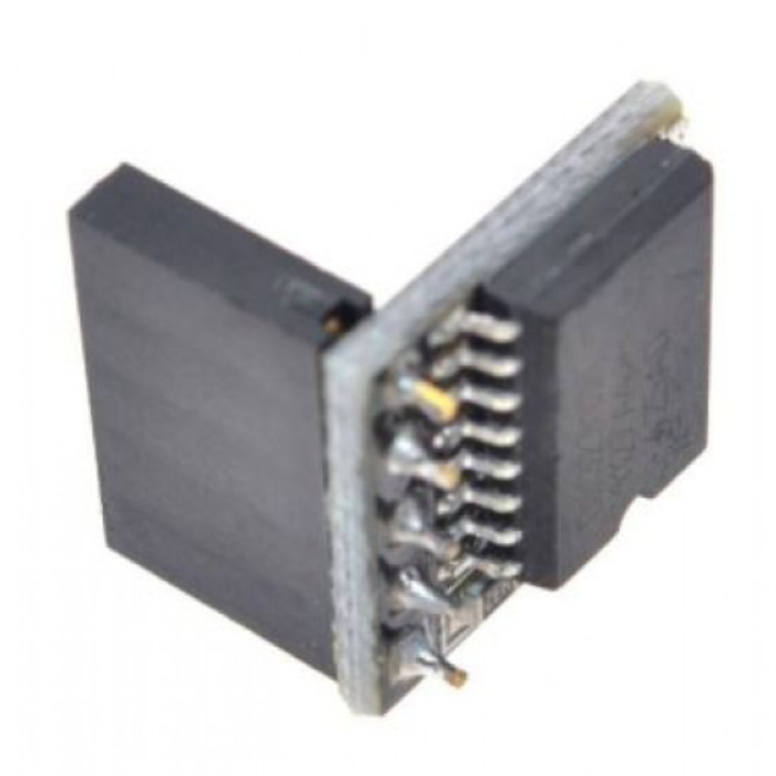
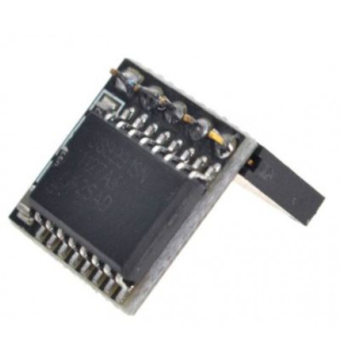
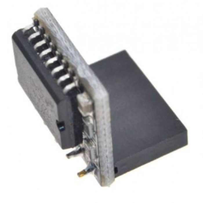
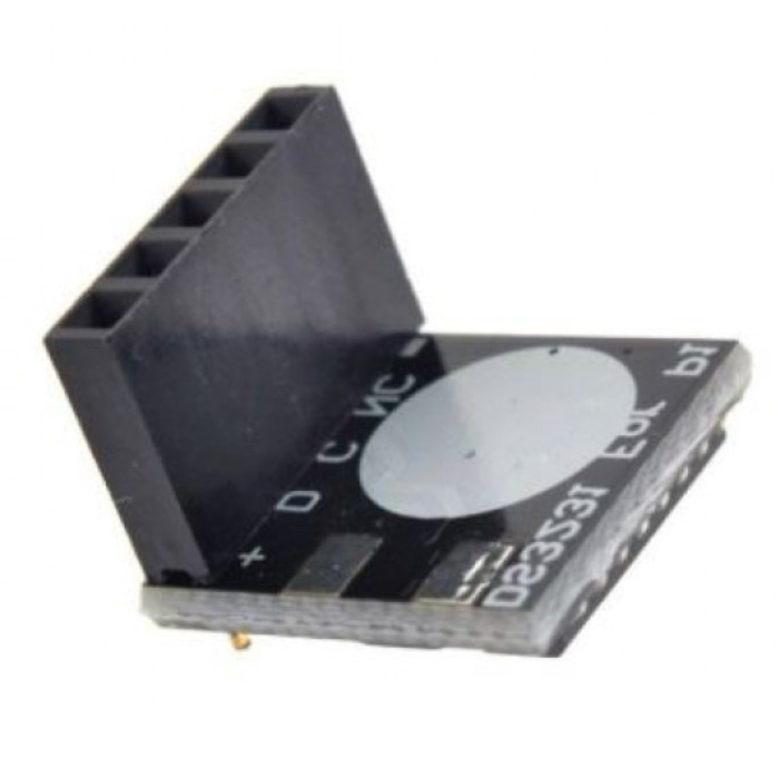
DS3231 Real Time Clock Module…
DS3231 Real Time Clock Module for Raspberry Pi (Without Battery)
The DS3231 Real-Time Clock (RTC) Module keeps accurate time for your Raspberry Pi and also works with Arduino. It tracks seconds, minutes, hours, day, date, month, and year, accurate up to the year 2100. The module adjusts to work with 3.3V or 5V, so it’s safe to use with Raspberry Pi. It has two alarms, a 1Hz and 32.768kHz output, and uses a fast I2C connection for easy setup. This low-power module also has a battery backup option (battery not included) to keep time when the main power is off.
₹186.39
Incl. GST (No Hidden Charges)
Backorder Available
₹348.60
Incl. GST (No Hidden Charges)


DS3231 Real Time Clock Module for Raspberry Pi (Without Battery)
DS3231 Real Time Clock Module for Raspberry Pi (Without Battery) The DS3231 Real-Time Clock (RTC) Module keeps accurate time for your Raspberry Pi and also works with Arduino. It tracks …
As low as
₹186.39
₹186.39
₹348.60
Incl. GST (No Hidden Charges)
Backorder Available
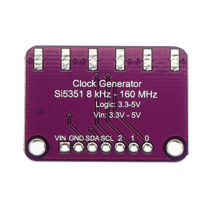
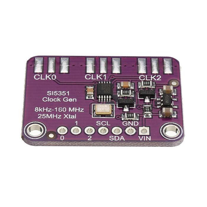
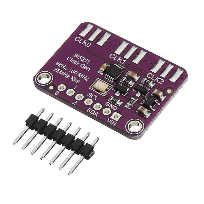
Si5351A Clock Signal Generato…
Si5351A Clock Signal Generator Module
The Si5351A
clock
generator is an I2C controller clock generator. It uses the onboard precision clock to drive multiple PLLs and clock dividers using I2C instructions. By setting up the PLL and dividers you can create precise and arbitrary frequencies. Outputs are 3Vpp, either through a breadboard-friendly header or, for RF work, an optional SMA connector.
Pinout:
Pinout Si5351A Clock Signal Generator Module
Applications
:
HDTV, DVD/Blu-ray, set-top box
Audio/video equipment, gaming
Printers, scanners, projectors
Residential gateways
Networking/communication
Servers, storage
XO replacement
₹278.52
Incl. GST (No Hidden Charges)
Backorder Available
₹488.60
Incl. GST (No Hidden Charges)
Si5351A Clock Signal Generator Module
Si5351A Clock Signal Generator Module The Si5351A clock generator is an I2C controller clock generator. It uses the onboard precision clock to drive multiple PLLs and clock dividers using I2C …
As low as
₹278.52
₹278.52
₹488.60
Incl. GST (No Hidden Charges)
Backorder Available
CD4015 - Dual 4-Stage Shift R…
CD4015 - Dual 4-Stage Shift Register IC
The CD4015
IC
consists of two identical, independent, 4-stage serial-input/parallel-output registers. Each register has independent CLOCK and RESET inputs as well as a single serial DATA input. “Q” outputs are available from each of the four stages on both registers. All register stages are D-type, master-slave flip-flops. The logic level present at the DATA input is transferred into the first register stage and shifted over one stage at each positive-going clock transition. Resetting of all stages is accomplished by a high level on the reset line. Register expansion to 8 stages using one CD4015 package, or to more than 8 stages using additional CD4015’s is possible.
The CD4015-series types are supplied in 16-lead hermetic dual-in-line ceramic packages (F3A suffix), 16-lead dual-in-line plastic package (E suffix), 16-lead small-outline packages (M, M96, MT, and NSR suffixes), and 16-lead thin shrink small-outline packages (PW and PWR suffixes).
check out :
CD4034 - 8-Stage Bidirectional Bus Register IC (Original)
Pinout:
Pinout Of CD4015 - Dual 4-Stage Shift Register IC
Pin Name
Pin #
Type
Description
VDD
16
Power
Supply Voltage (+3 to +15V)
GND
8
Power
Ground (0V)
D
A
7
Input
Data pin for register A
CLK
A
9
Input
Clock pulse for register A
RST
A
6
Input
Reset pin for register A
Q
A0
,Q
A1
,Q
A2
,Q
A3
5,4,3,10
Output
4-bit output for register A
D
B
15
Input
Data pin for register B
CLK
B
1
Input
Clock pulse for register B
RST
B
14
Input
Reset pin for register B
Q
B0
,Q
B1
,Q
B2
,Q
B3
11,12,13, 2
Output
4-bit output for register B
Applications:
Serial-input/parallel-output data queueing
Serial to parallel data conversion
General-purpose register
₹24.92
Incl. GST (No Hidden Charges)
Backorder Available
₹50.40
Incl. GST (No Hidden Charges)

CD4015 - Dual 4-Stage Shift Register IC
CD4015 - Dual 4-Stage Shift Register IC The CD4015 IC consists of two identical, independent, 4-stage serial-input/parallel-output registers. Each register has independent CLOCK and RESET inputs as well as a …
As low as
₹24.92
₹24.92
₹50.40
Incl. GST (No Hidden Charges)
Backorder Available
CD4059 - Programmable Divide-…
CD4059 - Programmable Divide-by-N Counter IC
The
CD4x Series
CD4059 standard "A" Series types are divide-by-N down-counters that can be programmed to divide an input frequency by any number "N" from 3 to 15,999. The output signal is a pulse one clock-cycle wide occurring at a rate equal to the input frequency divided by N. This single output has TTL drive capability. The down-counter is preset by means of 16 jam inputs.
The three Mode-Select Inputs Ka, Kb, and Kc determine the modulus ("divide-by" number) of the first and last counting sections. Every time the first (fastest) counting section goes through one cycle, it reduces by 1 the number that has been preset (jammed) into the three decades of the intermediate counting section and into the last counting section, which consists of flip-flops that are not needed for operating the first counting section.
For example, in the 2 modes, only one flip-flop is needed in the first counting section. Therefore the last counting section has three flip-flops that can be preset to a maximum count of seven with a place value of thousands. If 10 is desired for the first section, Ka is set to 1, Kb to 1, and Kc to 0. Jam Inputs J1, J2, J3, and J4 are used to preset the first counting section and there is no last counting section. The intermediate counting section consists of three cascaded BCD decade (10) counters presettable by means of Jam Inputs J5 through J16.
This device is particularly advantageous in communication digital frequency synthesis (VHF, UHF, FM, AM, etc.) where programmable divide-by-"N" counters are an integral part of the synthesizer phase-locked-loop sub-system. The CD4059 can also be used to perform the synthesizer "Fixed Divide-by-R" counting function. It is also useful in general-purpose counters for instrumentation functions such as totalizers, production counters, and "time-out" timers.
The CD4059B-series types are supplied in 24-lead dual-in-line plastic packages (E suffix), and 24-lead small-outline packages (M and M96 suffixes).
Pinout:
Pinout of CD4059 IC
Applications:
Communications digital frequency synthesizers: VHF, UHF, FM, AM, etc.
Fixed or programmable frequency division
"Time out" timer for consumer-application industrial controls
Companion Application Note, ICAN-6374, "Application of the CMOS CD4059A Programmable Divide-by-N Counter in FM and Citizens Band Transceiver Digital Tuners"
₹175.56
Incl. GST (No Hidden Charges)
Backorder Available
₹330.40
Incl. GST (No Hidden Charges)
CD4059 - Programmable Divide-by-N Counter IC
CD4059 - Programmable Divide-by-N Counter IC The CD4x Series CD4059 standard "A" Series types are divide-by-N down-counters that can be programmed to divide an input frequency by any number "N" …
As low as
₹175.56
₹175.56
₹330.40
Incl. GST (No Hidden Charges)
Backorder Available
CD4094 - 8-Stage Shift and St…
CD4094 - 8-Stage Shift and Store Bus Register IC
The CD4094
IC
belongs to the CD4000 IC series. This IC is composed of an 8-bit shift register and a 3- State 8-bit latch. In this IC, Data shifted serially through the shift register on the positive transition of the clock. The CD4082 IC operates at a wide range of working voltage, a wide range of working conditions. And directly interfaces with CMOS, NMOS, and TTL. The output of the IC always comes in TTL which makes it quite easy to function with other TTL devices and microcontrollers.
CD4094 offers features such as ESD barring and high noise immunity. Each output is protected against static damage by using clamping diodes. CD4094 Operates at a supply voltage of range between 3V to 20V. This IC is designed for operation over the full military temperature range of 0°C to 70°C. The IC CD4094 comes as smaller in size and offers much faster speed which makes it highly reliable in every kind of device. CD4094 IC can be soldered directly to the circuit board or easily mounted on a 16 pin IC base.
Shift-and-Store Bus Register is designed as a digital memory circuitry available in devices such as calculators, computers, and data processing systems. Using a Shift-and-Store Bus Register, data or bits enter into the system in a serial or parallel manner. Data entry is performed from one direction, and as more data is added, it shifts positions until the data gets to the output end. The two ends are referred to as the left and right ends. Whereas the movement of data occurs from left to right, from right to left. Or in both directions to make a bidirectional register.
check out :
CD4099 - 8 bit Addressable Latch IC
Pinout:
Pinout of CD4094 - 8-Stage Shift and Store Bus Register IC
Applications:
Serial-to-Parallel data conversion
Remote control holding register
Dual rank shift, hold, and bus register
₹23.84
Incl. GST (No Hidden Charges)
Backorder Available
₹47.60
Incl. GST (No Hidden Charges)

CD4094 - 8-Stage Shift and Store Bus Register IC
CD4094 - 8-Stage Shift and Store Bus Register IC The CD4094 IC belongs to the CD4000 IC series. This IC is composed of an 8-bit shift register and a 3- …
As low as
₹23.84
₹23.84
₹47.60
Incl. GST (No Hidden Charges)
Backorder Available
CD4013 - Dual D Type Flip-Flo…
CD4013 - Dual D Type Flip-Flop IC
The CD4013 designed as a CMOS logic chip IC belongs to the CD4XXX IC series. The CD4013 device comprises two identical, independent data-type flip-flops. Each flip-flop comes with independent data, set, reset, and clock inputs, and Q and Q’ outputs. These devices are commonly used for shift register applications, and, by connecting Q output to the data input, for counter and toggle applications. The logic level present at the D input is transmitted to the Q output during the positive-going transition of the clock pulse. Moreover, the Setting or resetting of IC is independent of the clock and accomplished by a high level on the set or reset line, respectively. The CD4013B is manufactured in 14-pin dual-inline plastic packages (E suffix), 14-pin small-outline packages (M, MT, M96, and NSR suffixes), and 14-pin thin shrink small-outline packages (PW and PWR suffixes).
A D-type Latch/flip-flop is designed as a
clocked latch that has two stable states. A D-type latch operates with a delay in input by one clock cycle. Thus, by cascading many D-type flip-flops delay circuits
are often
created, which are
utilized in
many applications
like
in digital television systems. A D-type flip-flop is additionally
mentioned
as a D flip-flop or a delay flip-flop. The D flip-flop is an edge-triggered device that transfers
input files
to Q on a clock rising or falling edge. Data Latches are level sensitive devices
like
the data
latch
and therefore the
transparent latch.
Applications
Power Delivery
Grid Infrastructure
Medical, Healthcare, and Fitness
Body Electronics and Lighting
Building Automation
Telecom Infrastructure
Test and Measurement
₹16.26
Incl. GST (No Hidden Charges)
Backorder Available
₹26.60
Incl. GST (No Hidden Charges)

CD4013 - Dual D Type Flip-Flop IC
CD4013 - Dual D Type Flip-Flop IC The CD4013 designed as a CMOS logic chip IC belongs to the CD4XXX IC series. The CD4013 device comprises two identical, independent data-type …
As low as
₹16.26
₹16.26
₹26.60
Incl. GST (No Hidden Charges)
Backorder Available
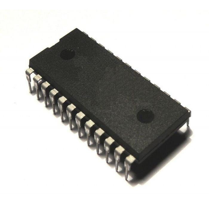
CD4017 - Decade Counter IC
CD4017 - Decade Counter IC
The CD4017
IC
is a
decade counter
that counts to ten. It has 10 outputs that represent the numbers 0 to 9. The counter increases with one for every rising clock pulse. After the counter has reached 9, it starts again from 0 with the next clock pulse.
This is a great chip for making running LEDs! See a circuit example further down.
check out :
Dual Complementary Pair with Inverter IC - CD4007
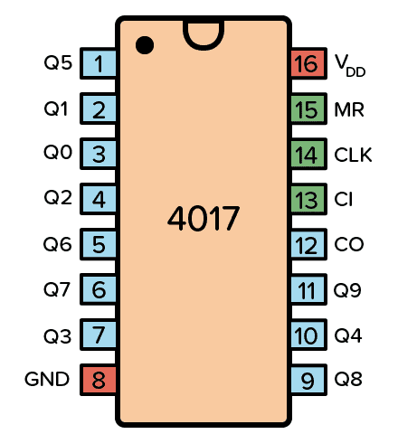
Pin Overview:
Pinout of CD4017 - Decade Counter IC
Pin Name
Pin #
Type
Description
VDD
16
Power
Supply Voltage (+3 to +15V)
GND
8
Power
Ground (0V)
Q0-Q9
1-7 and 9-11
Output
Qx is high when the counter is x
CO
12
Output
Carry Out. Goes high after ten clock pulses
CI
13
Input
Clock Inhibit. Ignores clock inputs
CLK
14
Input
Clock Input. Increases the counter with one
MR
15
Input
Resets the counter to 0
₹14.09
Incl. GST (No Hidden Charges)
Backorder Available
₹25.20
Incl. GST (No Hidden Charges)
CD4017 - Decade Counter IC
CD4017 - Decade Counter IC The CD4017 IC is a decade counter that counts to ten. It has 10 outputs that represent the numbers 0 to 9. The counter increases …
As low as
₹14.09
₹14.09
₹25.20
Incl. GST (No Hidden Charges)
Backorder Available
8-bit Up/Down Binary Counter …
8-bit Up/Down Binary Counter IC - CD40193
The CD40193 IC up/down counters are monolithic complementary MOS (CMOS) integrated circuits. The CD40192BM and CD40192BC are BCD counters, while the CD40193BM and CD40193BC are binary counters. Counting up and counting down is performed by two count inputs, one being held high while the other is clocked. The outputs change on the positive-going transition of this clock.
These
CD4x Series IC
counters feature preset inputs that are enabled when the load is a logical ‘‘0’’ and a clear which forces all outputs to ‘‘0’’ when it is at a logical ‘‘1’’. The counters also have to carry and borrow outputs so that they can be cascaded using no external circuitry. All inputs are protected against damage due to static discharge by clamps to VDD and VSS.
check out :
Divide by 8 Counter/Divider IC - CD4022
Pinout:
Pinout of CD40193 IC
Application
Up/Down difference counting
Multistage ripple counting
Synchronous frequency divider
A/D or D/A conversion
BCD counting
₹61.77
Incl. GST (No Hidden Charges)
Backorder Available
₹96.60
Incl. GST (No Hidden Charges)
8-bit Up/Down Binary Counter IC - CD40193
8-bit Up/Down Binary Counter IC - CD40193 The CD40193 IC up/down counters are monolithic complementary MOS (CMOS) integrated circuits. The CD40192BM and CD40192BC are BCD counters, while the CD40193BM and …
As low as
₹61.77
₹61.77
₹96.60
Incl. GST (No Hidden Charges)
Backorder Available
