Triple 3-Input NAND Gate IC - CD4023
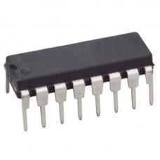
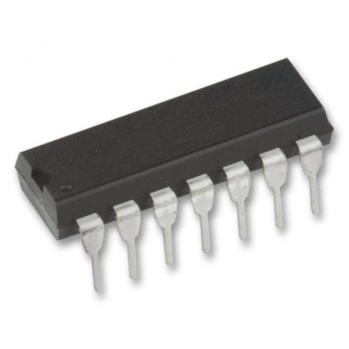
Triple 3-Input NAND Gate IC - CD4023 The Triple 3-Input CD4023 IC belongs to the CD4000 IC series. It consists of three NAND gates with 3 inputs and 1 unified output. The CD4x Series CD4023 is constructed by using the complementary MOS (CMOS) technology, integrated with p-type and n-type enhancement mode transistors. The IC also has buffered outputs which improve transfer characteristics by providing very high gain. All inputs are protected against static discharge with diodes to VDD and VSS. The IC offers a wide variety of working conditions, and a wide range of operating voltages, and directly interfaces with other TTL, CMOS, and NMOS devices. CD4023 always comes in a 14–pin hermetically sealed dual inline package (DIP). The IC also offers many additional features such as high noise immunity and ESD barring. check out : Triple 3-Input AND Gate IC - CD4073 Pinout: Pinout of CD4023 IC Pin Name Pin # Type Description VDD 14 Power Supply Voltage (+3 to +15V) GND 7 Power Ground (0V) A1 to A3 1, 3, 11 Input Inputs A of the three NAND gates B1 to B3 2, 4, 12 Input Inputs B of the three NAND gates C1 to C3 8, 5, 13 Input Inputs C of the three NAND gates Q1 to Q3 9, 6, 10 Output Outputs from the three NAND gates Application Burglar alarm Freezer warning buzzer A light-activated burglar alarm A push-button lock Package Includes: 1 x IC - CD4023 Specifications: Part number CD4023B Technology Family CD4000 VCC (Min) (V) 3 VCC (Max) (V) 18 Channels (#) 4 Inputs per channel 2 IOL (Max) (mA) 1.5 IOH (Max) (mA) -1.5 Input type Standard CMOS Output type Push-Pull Features Standard Speed (tpd > 50ns) Rating See Data Sheet Data rate (Max) (Mbps) 8 Operating temperature range (C) -55 to 125 Package size: mm2:W x L (PKG) 14PDIP: 181 mm2: 9.4 x 19.3 (PDIP|14) Package Group PDIP|14
- Propagation delay time = 60 ns (typ.) at CL = 50 pF, VDD = 10 V
- Buffered inputs and outputs
- Standardized symmetrical output characteristics
- Maximum input current of 1 µA at 18 V over-full package temperature range; 100 nA at 18 V and 25°C
- 100% tested for quiescent current at 20 V
- 5-V, 10-V, and 15-V parametric ratings
- Noise margin (over full package temperature range: 1 V at VDD = 5 V 2 V at VDD = 10 V 2.5 at VDD = 15 V
- Meets all requirements of JEDEC Tentative Standard No. 13B, "Standard Specifications for Description of "B" Series CMOS Devices".
- 1 x IC - CD4023
- Part number CD4023B
- Technology Family CD4000
- VCC (Min) (V) 3
- VCC (Max) (V) 18
- Channels (#) 4
- Inputs per channel 2
- IOL (Max) (mA) 1.5
- IOH (Max) (mA) -1.5
- Input type Standard CMOS
- Output type Push-Pull
- Features Standard Speed (tpd > 50ns)
- Rating See Data Sheet
- Data rate (Max) (Mbps) 8
- Operating temperature range (C) -55 to 125
- Package size: mm2:W x L (PKG) 14PDIP: 181 mm2: 9.4 x 19.3 (PDIP|14)
- Package Group PDIP|14