(0)
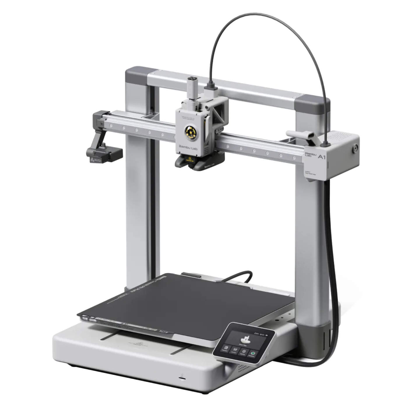
Bambu Lab A1 Combo 3D Printer with AMS Lite for Multi-Colour 3D Printing
The
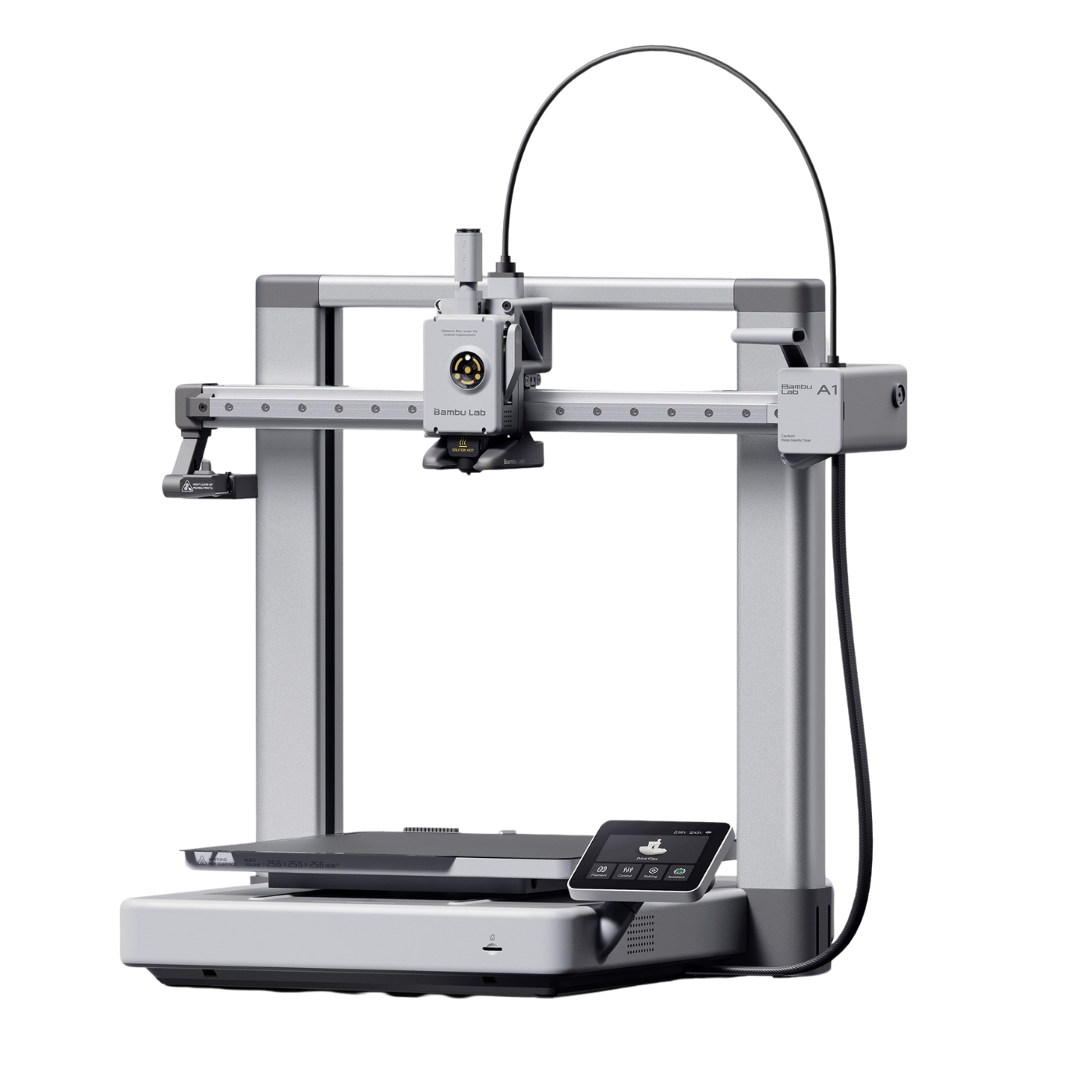
Bambu Lab A1 Combo is an advanced 3D printer
includes the AMS lite for smooth
multi-color 3D printing
. It features full
auto calibration
,
active flow rate compensation
, and a
quick-swap nozzle
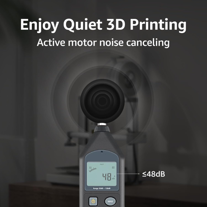
system for easy maintenance. With active noise-canceling motors, it runs quietly while delivering high-quality results. The A1 Combo
3D printer machine
offers a generous 256×256×256 mm³ build volume and
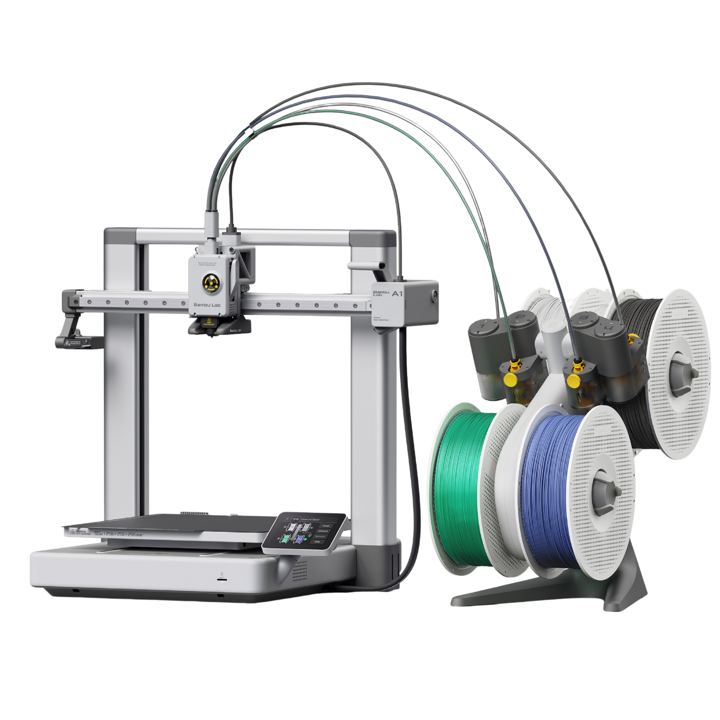
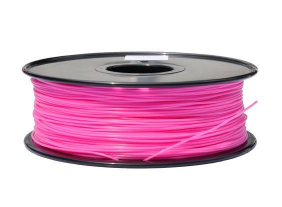
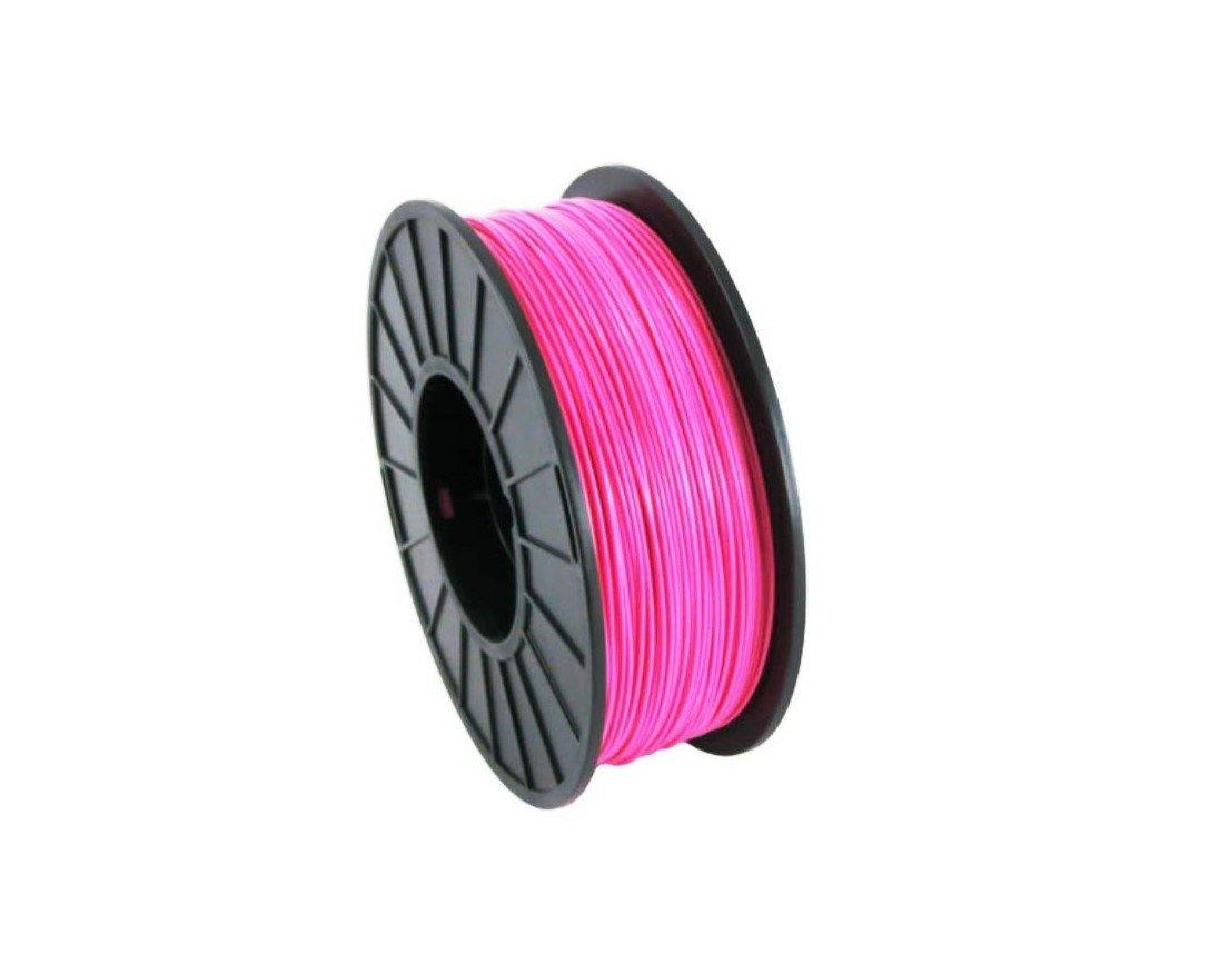
supports a range of filaments like PLA, PETG, and TPU
.
Features
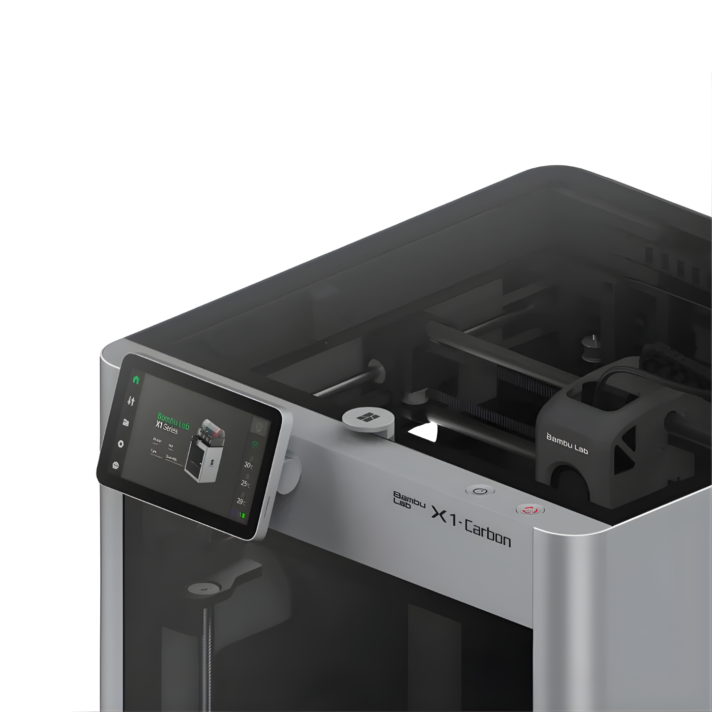
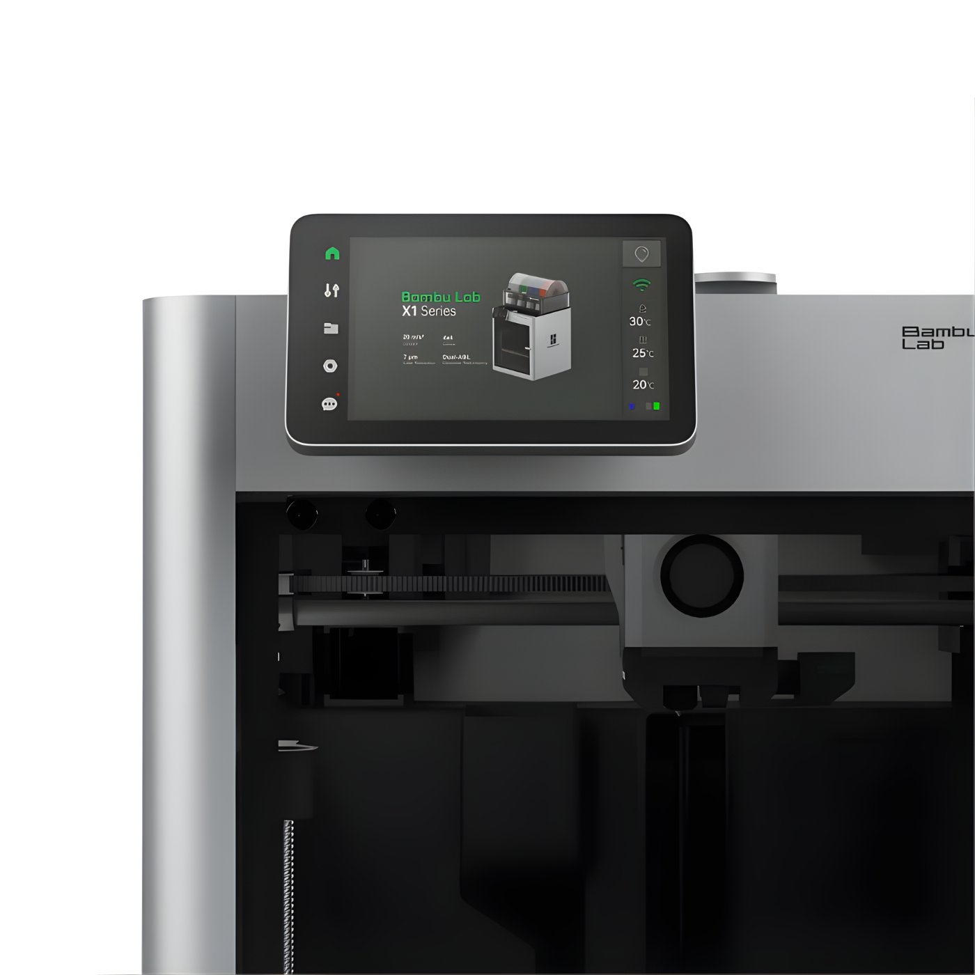
Intuitive Touchscreen Interface
Designed for simplicity, the
Bambu Lab
A1 Combo features a smartphone-like touchscreen UI that makes operation easy, even for beginners.
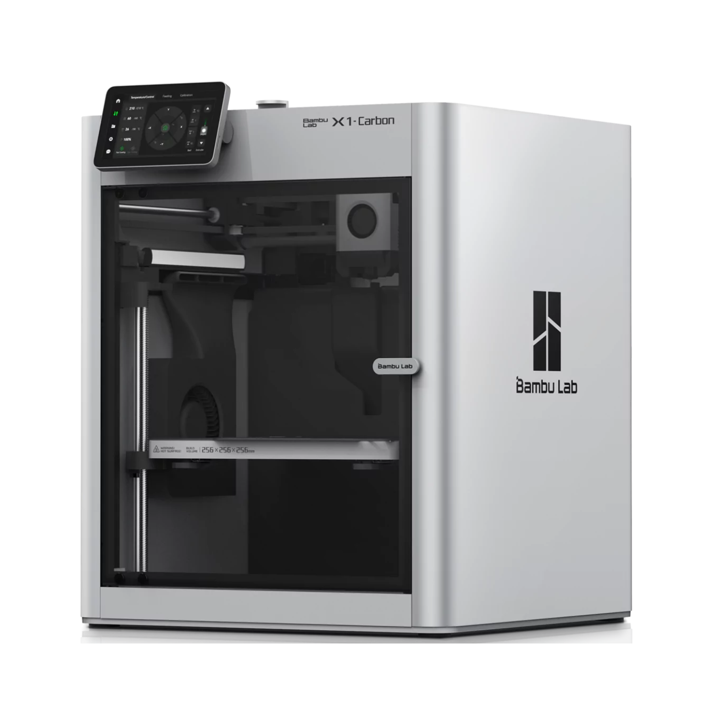
High-Speed Precision Printing
Combining a bed-slinger design with CoreXY-like speed and quality, the A1 3D printer uses full-metal rails, a rigid frame, nozzle pressure sensors, accelerometers, and a powerful MCU to achieve fast, precise prints—capable of printing a Benchy in just 14 minutes.
Active Flow Rate Compensation
With a high-resolution eddy current sensor, the Bambu Lab A1 Combo precisely monitors and adjusts flow rates during printing for smooth, accurate extrusion, ensuring flawless details on every corner.
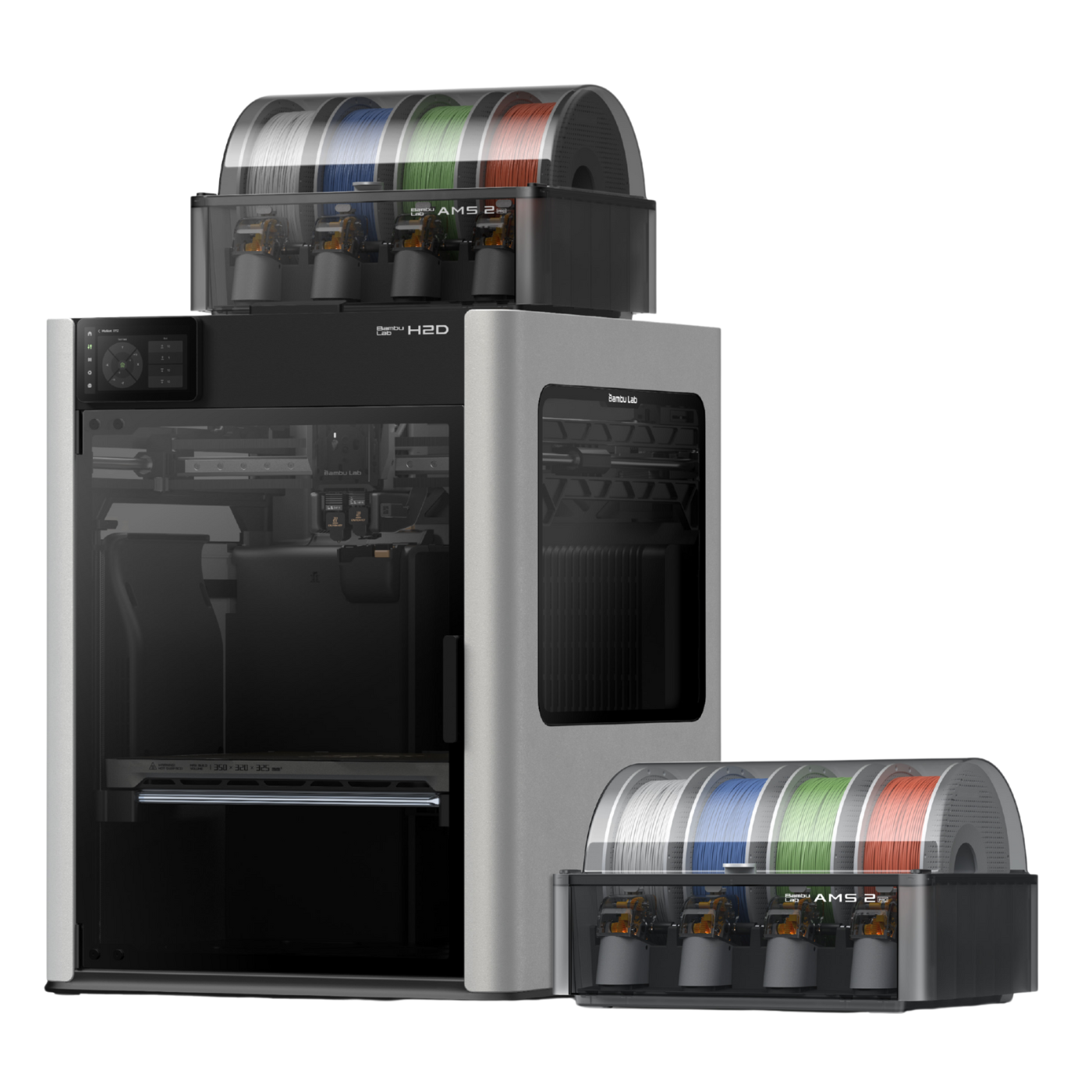
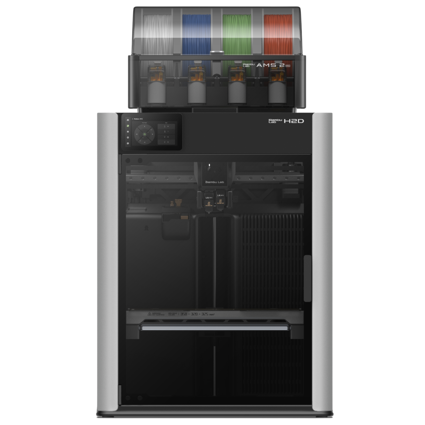
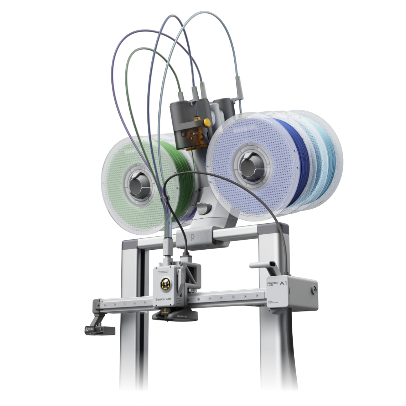
AMS Lite for Multi-Colour Printing
The included
Bambu Lab AMS Lite
system brings hassle-free multi-colour 3D printing to everyone, offering reliable and user-friendly performance.
1-Touch Filament Loading/Unloading
Forget manual
filament
handling—A1 automates filament loading and unloading with a simple touch.
Auto Belt Monitoring and Adjustment
The Bambu Lab A1 Combo 3D printer automatically checks belt tension and alerts users if adjustments are needed, ensuring optimal performance through its HMS (Health Management System).
Full-Auto Calibration
From bed levelling to vibration resonance, Z-offset, and nozzle pressure, the A1 3D printing machine fully automates calibration before every print for maximum reliability and quality.
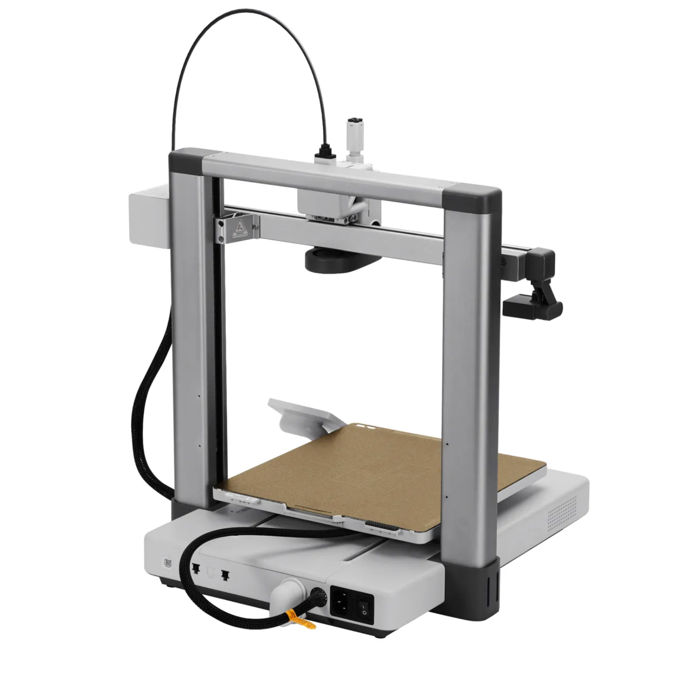
Durable, All-Metal Construction
Built with all-metal rails, bearings, and frame, the A1 is engineered for long-lasting reliability and consistent results.
MakerWorld & 1-Click Printing
Seamlessly print from MakerWorld, Bambu Lab’s next-gen 3D printing model platform, with 1-click printing via the
Bambu Handy App
or manage prints easily using Bambu Studio and the Handy App anytime, anywhere.
₹52297.67
MRP. ₹76998.60
Incl. GST (No Hidden Charges)