My Menu
CMOS Hex Buffers/Converter IC - CD4009
(0)
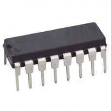
CMOS Hex Buffers/Converter IC - CD4009 CD4009 Hex Buffer/Converters may be used as CMOS to TTL or DTL logic-level converters or CMOS high-sink-current drivers. The CD4009 types are supplied in 16-lead hermetic dual-in-line ceramic packages (F3A suffix), 16-lead dual-in-line plastic packages (E suffix). check out : CMOS 8-Input NAND/AND Gate IC - CD4068 Applications: CMOS to DTL/TTL hex converter CMOS current "sink" or "source" driver CMOS high-to-low logic-level converter Multiplexer — 1 to 6 or 6 to 1 check out : Hex Buffer/Converter IC - CD4010 Package Includes: Selected qty of IC - CD4009 Specifications: Part number CD4009UB Technology Family …
As low as ₹27.06 ₹33.82 Incl. GST (No Hidden Charges)
IN STOCK
For bulk orders or wholesale inquiries, please contact us at iotcart.help@gmail.com or call/message us at +918050206487.

CMOS Hex Buffers/Converter IC - CD4009 CD4009 Hex Buffer/Converters may be used as CMOS to TTL or DTL logic-level converters or CMOS high-sink-current drivers. The CD4009 types are supplied in 16-lead hermetic dual-in-line ceramic packages (F3A suffix), 16-lead dual-in-line plastic packages (E suffix). check out : CMOS 8-Input NAND/AND Gate IC - CD4068 Applications: CMOS to DTL/TTL hex converter CMOS current "sink" or "source" driver CMOS high-to-low logic-level converter Multiplexer — 1 to 6 or 6 to 1 check out : Hex Buffer/Converter IC - CD4010 Package Includes: Selected qty of IC - CD4009 Specifications: Part number CD4009UB Technology Family CD4000 Bits (#) 6 Voltage (Nom)(V)        5 IOH (Max)(mA) -1.1 IOL (Max)(mA) 16 F@nom voltage (Max)(MHz) 12 ICC@nom voltage (Max)(mA) 0.03 Schmitt trigger No tpd@nom Voltage (Max) (ns) 140 Rating See Data Sheet Package Group PDIP|16

  • 100% tested for quiescent current at 20 V
  • Maximum input current of 1 µA at 18 V over full package-temperature range; 100 nA at 18 V and 25°C
  • 5-V, 10-V, and 15-V parametric ratings
To rate this product please login!

Related products

Related products

Decade Counter/Divider IC - CD4026 20%
Decade Counter/Divider IC - C…
(0)
Decade Counter/Divider IC - CD4026 The CD4x Series CD4026 consists of a 5-stage Johnson decade counter and an output decoder that converts the Johnson code to a 7-segment decoded output for driving one stage in a numerical display. These devices are particularly advantageous in display applications where low power dissipation and /or low package count are important. Inputs common to both types are CLOCK, RESET, & CLOCK INHIBIT; common outputs are CARRY OUT and the seven decoded outputs (a, b, c, d, e, f, g). Additional inputs and outputs for the CD4026 include DISPLAY ENABLE input and DISPLAY ENABLE and UNGATED "C-SEGMENT" outputs.  A high RESET signal clears the decade counter to its zero counts. The counter is advanced one count at the positive clock signal transition if the CLOCK INHIBIT signal is low. Counter advancement via the clock line is inhibited when the CLOCK INHIBIT signal is high. The CLOCK INHIBIT signal can be used as a negative-edge clock if the clock line is held high. Antilock gating is provided on the JOHNSON counter, thus assuring proper counting sequence. The CARRY-OUT (Cout) signal completes one cycle every ten CLOCK INPUT cycles and is used to clock the succeeding decade directly in a multi-decade counting chain. The seven decoded outputs (a, b, c, d, e, f, g) illuminate the proper segments in a seven-segment display device used for representing the decimal numbers 0 to 9. The CD4026  outputs go high only when the DISPLAY ENABLE IN is high. The CD4026 series type is supplied in 16-lead dual-in-line plastic packages (E suffix), 16-lead small-outline packages (NSR suffix), and 16-lead thin shrink small-outline packages (PW and PWR suffixes). check out : CD4033 - 5-Stage Johnson Decade counter IC Pinout: Pinout of CD4026 Decade IC Applications: Decade counting 7-segment decimal display Frequency division 7-segment decimal displays Clocks, watches, timers (e.g. ÷60, ÷60, ÷ 12 counter/display) Counter/display driver for meter applications Package Includes: Selected qty of IC - CD4026 Specifications: Part number CD4026B Technology Family CD4000 VCC (Min) (V) 3 VCC (Max) (V) 18 Bits (#) 7 Voltage (Nom) (V) 5, 10, 15 F @ nom voltage (Max) (MHz) 8 ICC @ nom voltage (Max) (mA) 0.03 tpd @ nom Voltage (Max) (ns) 250 IOL (Max) (mA) 1.5 IOH (Max) (mA) -1.5 Function Counter Type Decade Rating See Data Sheet Operating temperature range (C) -55 to 125 Package Group PDIP|16
₹35.71 ₹44.64 Incl. GST
Hex Buffer/Converter IC - CD4010 20%
Hex Buffer/Converter IC - CD4…
(0)
Hex Buffer/Converter IC - CD4010 The CD4010C hex buffers IC are monolithic complementary MOS (CMOS) integrated circuits. The N- and P-channel enhancement mode transistors provide a symmetrical circuit with output swings essentially equal to the supply voltage. This results in high noise immunity over a wide supply voltage range. No DC power other than that caused by leakage current is consumed during static conditions. All inputs are protected against static discharge. These gates may be used as hex buffers, CMOS to DTL or TTL interface or as CMOS current drivers. Conversion ranges are from 3V to 15V providing VCC ≤ VDD. The devices also have buffered outputs which improve transfer characteristics by providing very high gain. The CD4x Series CD4010 Hex Buffer/Converters may be used as CMOS to TTL or DTL logic-level converters or CMOS high-sink-current drivers. The CD4010 types are supplied in 16-lead hermetic dual-in-line ceramic packages (F3A suffix), and 16-lead dual-in-line plastic packages (E suffix). check out : CD4050 - Hex Non-Inverting Buffer IC Applications: CMOS to DTL/TTL hex converter CMOS current "sink" or "source" driver CMOS high-to-low logic-level converter Multiplexer — 1 to 6 or 6 to 1 Package Includes: 1 x IC - CD4010 Specifications: Part number CD4010B Technology Family CD4000 Bits (#) 6 Voltage (Nom) (V) 10 IOH (Max)(mA) -1.65 IOL(Max)(mA) 30 F @ nom voltage (Max)(MHz) 8 ICC @ nom voltage (Max)(mA) 0.06 Schmitt trigger No tpd @ nom Voltage (Max)(ns) 200 Rating See Data Sheet Package Group PDIP|16
₹25.98 ₹32.47 Incl. GST
CD4052 - Differential 4-channel Multiplexer/Demultiplexer IC 20%
CD4052 - Differential 4-chann…
(0)
CD4052 - Differential 4-channel Multiplexer/Demultiplexer IC The CD4052 analog multiplexers/demultiplexers IC are digitally controlled analog switches having low “ON” impedance and very low “OFF” leakage currents. Control of analog signals up to 15Vp-p can be achieved by digital signal amplitudes of 3−15V. For example, if VDD = 5V, VSS = 0V and VEE = −5V, analog signals from −5V to +5V can be controlled by digital inputs of 0−5V. The multiplexer circuits dissipate extremely low quiescent power over the full VDD−VSS and VDD−VEE supply voltage ranges, independent of the logic state of the control signals. When a logical “1” is present at the inhibit input terminal all channels are “OFF”. CD4052 is a differential 4-channel multiplexer having two binary control inputs, A and B, and an inhibit input. The two binary input signals select 1 or 4 pairs of channels to be turned on and connect the differential analog inputs to the differential outputs. Pinout: Pinout of CD4052 - Differential 4-channel Multiplexer/Demultiplexer IC  Pin Number Pin Name Description 16 Vdd Positive power input, maximum 20V 7 Vee Negative power rail, normally connected to ground. 8 Vss (Ground) Connected to ground of the circuit  6 INH Enable pin – Must be pulled to ground for normal operation 9,10 A,B Channel Select pins 1,12 Y0,X0 Channel 0 Input / Output 5,14 Y1,X1 Channel 1 Input / Output 2,15 Y2,X2 Channel 2 Input / Output 4,11 Y3,X3 Channel 3 Input / Output 3,13 Y,X Common Output / Input Package Includes: 1 x IC - CD4052 Specifications: Part number CD4052BC DC Supply Voltage (VDD) −0.5 VDC to +18 VDD Input Voltage (VIN) −0.5 VDC to VDD +0.5 VDC  Storage Temperature Range (TS) −65°C to +150°C   Power Dissipation (PD) Dual-In-Line 700 mW Lead Temperature (TL) 260°C
₹17.31 ₹21.64 Incl. GST
CD4011 - Quad 2-Input NAND Gate IC 20%
CD4011 - Quad 2-Input NAND Ga…
(0)
CD4011 - Quad 2-Input NAND Gate IC The CD4011 is a quad package 2-Input NAND gate IC(Integrated Circuits). That is, it has four NAND gates inside a single package and each gate has two input lines and one output line. All the inputs and outputs are buffered and this improves transfer characteristics by providing a very high gain. The CD4011 IC operates at 5V, 10V, 15V, and even 20V. When operating at 5V the maximum low-level input voltage is 0.5 and the minimum high-level input voltage is 4.5. All four gates share the same power rail but can operate independently. Pinout: Pinout Of CD4011 IC PACKAGE INCLUDES: Selected qty of IC - CD4011 Specifications: Operating Voltage 5V Low-Level Output Current 1.5mA Propagation Delay Time 60ns Operating Temperature Range - 55 C to + 125 C
₹20.57 ₹25.71 Incl. GST
CD4030 - Quad 2-Input Exclusive OR (EXOR) Gate IC 20%
CD4030 - Quad 2-Input Exclusi…
(0)
CD4030 - Quad 2-Input Exclusive OR (EXOR) Gate IC The CD4030 IC types consist of four independent Exclusive-OR gates. The CD4030 provides the system designer with a means for direct implementation of the Exclusive-OR function. The CD4030 types are supplied in 14-lead hermetic dual-in-line ceramic packages (F3A suffix), 14-lead dual-in-line plastic packages (E suffix), 14-lead small-outline packages (M, MT, M96, and NSR suffixes), and 14-lead thin shrink small-outline packages (PW and PWR suffixes). check out : CD4519 - Quad AND/OR Select Gate IC (Original) Pinout: Pinout of CD4030 - Quad 2-Input Exclusive OR (EXOR) Gate IC Applications: Even and odd-parity generators and checkers Logical comparators Adders/subtractors General logic functions check out : CD4081 - Quad 2 Input AND Gate IC Package Includes: Selected qty of IC - CD4030 Specifications: Part number CD4030B Technology Family CD4000 VCC (Min) (V) 3 VCC (Max) (V) 18 Channels (#) 4 Inputs per channel 4 IOL (Max) (mA) 6.8 Input type Standard CMOS IOH (Max) (mA) -6.8 Output type Push-Pull Features Standard Speed (tpd > 50ns) Data rate (Max) (Mbps) 8 Rating See Data Sheet Operating temperature range (C) -55 to 125 Package size: mm2:W x L (PKG) 14PDIP: 181 mm2: 9.4 x 19.3 (PDIP|14) Package Group PDIP|14
₹23.81 ₹29.76 Incl. GST
16-Channel Analog Multiplexer/Demultiplexer IC - CD4067 20%
16-Channel Analog Multiplexer…
(0)
16-Channel Analog Multiplexer/Demultiplexer IC - CD4067 CD4067 CMOS analog multiplexers/demultiplexers are digitally controlled analog switches having low ON impedance, low OFF leakage current, and internal address decoding. In addition, the ON resistance is relatively constant over the full input-signal range. The CD4067 is a 16-channel multiplexer with four binary control inputs, A, B, C, D, and an inhibit input, arranged so that any combination of the inputs selects one switch. A logic “1” present at the inhibit input turns all channels off. The CD4067 type are supplied in 24-lead hermetic dual-in-line ceramic packages (F3A suffix), 24-lead dual-in-line plastic packages (E suffix), 24-lead small-outline packages (M, M96, and NSR suffixes), and 24-lead thin shrink small-outline packages (P and PWR suffixes). check out : CD4066 - Quad Bilateral Switch IC Applications: Analog and digital multiplexing and demultiplexing A/D and D/A conversion Signal gating Package Includes: Selected qty of IC - CD4067 Specifications: Part number CD4067 Configuration 16:01 Number of channels (#) 1 Ron (Typ) (Ohms) 125 Bandwidth (MHz) 14 Rating Catalog Operating temperature range (C) -55 to 125 Package Group PDIP|24 Input/output continuous current (Max (mA) 10 Supply current (Typ (uA) 0.04 CON (Typ) (pF) 5
₹172.07 ₹215.09 Incl. GST
CD4016 - Quad Bilateral Switch IC 20%
CD4016 - Quad Bilateral Switc…
(0)
CD4016 - Quad Bilateral Switch IC The CD4x Series CD4016 is a quad bilateral switch intended for the transmission or multiplexing of analog or digital signals. It is pin-for-pin compatible with CD4066B.  The CD4016 is a CMOS IC with four analog switches, which can be controlled individually using a control pin. The signal can flow in either direction between the two pins of each switch. Each switch has an enable pin (A) and two input/output pins (X and Y). When the enable pin is set to HIGH, current can flow between X and Y in either direction. However, when enable is LOW, no current can flow between the pins. Just like a switch. Pinout: Pinout of CD4016 IC Pin Name Pin # Type Description VDD 14 Power Supply Voltage (+3 to +15V) GND 7 Power Ground (0V) A1-A4 5,6,12,13 Input Enable pins for the four bilateral switches X1-X4 1,3,9,11 Input/Output Pin X for each switch Y1-Y4 2,4,8,10 Input/Output Pin Y for each switch Package Includes: Selected qty of IC - CD4016 Specifications: VDD Supply Voltage −0.5V to +18V VIN Input Voltage −0.5V to VDD + 0.5V TS Storage Temperature Range  −65°C to + 150°C Power Dissipation (PD): Dual-In-Line 700 mW Lead Temperature 260°C
₹22.73 ₹28.40 Incl. GST
CD4532 - 8 Bit Priority Encoder IC (Original) 20%
CD4532 - 8 Bit Priority Encod…
(0)
CD4532 - 8 Bit Priority Encoder IC The CD4x Series CD4532 consists of combinational logic that encodes the highest priority input (D7-D0) to a 3-bit binary code. The eight inputs, D7 through D0, each have an assigned priority; D7 is the highest priority and D0 is the lowest. The priority encoder is inhibited when the chip-enable input EI is low. When EI is high, the binary representation of the highest-priority input appears on output lines Q2-Q0, and the group select line GS is high to indicate that priority inputs are present. The enable-out (EO) is high when no priority inputs are present. If any one input is high, EO is low and all cascaded lower-order stages are disabled. The CD4532 types are supplied in 16-lead hermetic dual-in-line ceramic packages (F3A suffix), 16-lead dual-in-line plastic packages (E suffix), 16-lead small-outline packages (M, M96, MT, and NSR suffixes), and 16-lead thin shrink small-outline packages (PW and PWR suffixes). Pinout: Pinout of CD4532 IC Applications: Priority encoder Binary or BCD encoder (keyboard encoding) Floating-point arithmetic Package Includes: Selected qty of IC - CD4532 Specifications: Part number CD4532B Technology Family CD4000 VCC (Min) (V) 3 VCC (Max) (V) 18 Channels (#) 1 Voltage (Nom) (V) 5, 10, 15 F @ nom voltage (Max) (MHz) 8 ICC @ nom voltage (Max) (mA) 0.3 tpd @ nom Voltage (Max) (ns) 110 IOL (Max) (mA) 1.5 IOH (Max) (mA) -1.5 Function Encoder Type Standard Operating temperature range (C) -55 to 125 Package Group PDIP|16 Configuration 08:04 Bits (#) 8 Digital input leakage (Max (uA) 5 ESD CDM (kV) 0.75 ESD HBM (kV) 2
₹43.29 ₹54.11 Incl. GST
Divide by 8 Counter/Divider IC - CD4022 20%
Divide by 8 Counter/Divider I…
(0)
Divide by 8 Counter/Divider IC - CD4022 The CD4022 IC is a 4-stage divide-by-8 Johnson counter with 8 decoded outputs and a carry-out bit. These counters are cleared to their zero counts by a logical ‘‘1’’ on their reset line. These counters are advanced on the positive edge of the clock signal when the clock enable signal is in the logical ‘‘0’’ state. The configuration of the CD4x Series CD4022 permits medium-speed operation and assures a hazard-free counting sequence. The 10/8 decoded outputs are normally in the logical ‘‘0’’ state and go to the logical ‘‘1’’ state only at their respective time slot. Each decoded output remains high for 1 full clock cycle. The carry-out signal completes a full cycle for every 10/8 clock input cycle and is used as a ripple to carry the signal to any succeeding stages. check out : 8-bit Up/Down Binary Counter IC - CD40193 Pinout: Pinout of CD4022 IC Package Includes: 1 x IC - CD4022 Specifications: DC Supply Voltage (VDD)  -0.5 VDC to + 8 VDC  Input Voltage (VIN)   -0.5 VDC to VDD +0.5 VDC  Storage Temperature (TS)   -65°C to +150°C  Power Dissipation (PD) Dual-In-Line  700 mW Lead Temperature (TL)   260°C
₹20.57 ₹25.71 Incl. GST
CD4094 - 8-Stage Shift and Store Bus Register IC 20%
CD4094 - 8-Stage Shift and St…
(0)
CD4094 - 8-Stage Shift and Store Bus Register IC The CD4094 IC belongs to the CD4000 IC series. This IC is composed of an 8-bit shift register and a 3- State 8-bit latch. In this IC, Data shifted serially through the shift register on the positive transition of the clock. The CD4082 IC operates at a wide range of working voltage, a wide range of working conditions. And directly interfaces with CMOS, NMOS, and TTL. The output of the IC always comes in TTL which makes it quite easy to function with other TTL devices and microcontrollers. CD4094 offers features such as ESD barring and high noise immunity. Each output is protected against static damage by using clamping diodes. CD4094 Operates at a supply voltage of range between 3V to 20V. This IC is designed for operation over the full military temperature range of 0°C to 70°C. The IC CD4094 comes as smaller in size and offers much faster speed which makes it highly reliable in every kind of device. CD4094 IC can be soldered directly to the circuit board or easily mounted on a 16 pin IC base. Shift-and-Store Bus Register is designed as a digital memory circuitry available in devices such as calculators, computers, and data processing systems. Using a Shift-and-Store Bus Register, data or bits enter into the system in a serial or parallel manner. Data entry is performed from one direction, and as more data is added, it shifts positions until the data gets to the output end. The two ends are referred to as the left and right ends. Whereas the movement of data occurs from left to right, from right to left. Or in both directions to make a bidirectional register. check out : CD4099 - 8 bit Addressable Latch IC Pinout: Pinout of CD4094 - 8-Stage Shift and Store Bus Register IC Applications: Serial-to-Parallel data conversion Remote control holding register Dual rank shift, hold, and bus register Package Includes: 1 x IC - CD4094 Specification: High Voltage Type 20V Medium Speed Operation 5MHz at 10V (typ) Maximum Input Current 1µA at 18V Parametric Ratings 5V, 10V and 15V Dimensions 7x4x3mm Weight 2g
₹22.73 ₹28.40 Incl. GST
CD4017 - Decade Counter IC 20%
CD4017 - Decade Counter IC
(0)
CD4017 - Decade Counter IC The CD4017 IC is a decade counter that counts to ten. It has 10 outputs that represent the numbers 0 to 9. The counter increases with one for every rising clock pulse. After the counter has reached 9, it starts again from 0 with the next clock pulse. This is a great chip for making running LEDs! See a circuit example further down. check out : Dual Complementary Pair with Inverter IC - CD4007 Pin Overview: Pinout of CD4017 - Decade Counter IC Pin Name Pin # Type Description VDD 16 Power Supply Voltage (+3 to +15V) GND 8 Power Ground (0V) Q0-Q9 1-7 and 9-11 Output Qx is high when the counter is x CO 12 Output Carry Out. Goes high after ten clock pulses CI 13 Input Clock Inhibit. Ignores clock inputs CLK 14 Input Clock Input. Increases the counter with one MR 15 Input Resets the counter to 0 Package Includes: Selected qty of IC - CD4017 Specifications: Input Voltage (VIN)  −0.5 VDC to VDD +0.5 VDC  Storage Temperature (TS)  −65°C to +150°C DC Supply Voltage (VDD)  −0.5 VDC to +18 VDC Power Dissipation (PD): Dual-In-Line  700 mW Lead Temperature (TL)   260°C
₹12.99 ₹16.24 Incl. GST
CD40106 - Hex Schmitt Trigger Inverter IC 20%
CD40106 - Hex Schmitt Trigger…
(0)
CD40106 - Hex Schmitt Trigger Inverter IC  The CD40106 IC consists of six Schmitt-Trigger inputs. Each circuit functions as an inverter with Schmitt-Trigger input. The trigger switches at different points for positive- and negative-going signals. The difference between the positive-going voltage (VP) and the negative-going voltage (VN) is defined as hysteresis voltage (VH). A Schmitt trigger input means that the threshold voltage for going from a HIGH to a LOW input is different from the threshold for going from LOW to HIGH. CD40106 Pinout Configuration: Pin Number Pin Name Description 1,3,5,11,13,15 Schmitt Input Pins Input pins of the Schmitt trigger 2,4,6,10,12,14 Schmitt Inverted Output Pins Output pins of the Schmitt trigger 7 Ground Connected to the ground of the system 14 Vcc (+5V) Resets all outputs as low. Must be held high for normal operation Applications of CD40106: Noise removing circuits Debouncing circuits Hysteresis controller Dead band filter Package Includes: 1 x IC - CD40106 Specifications: Schmitt Trigger Hex Inverter Operating Voltage 5V Low-Level Hysteresis voltage 0.3V High-Level Hysteresis voltage 3.5V
₹21.64 ₹27.06 Incl. GST
CD4519 - Quad AND/OR Select Gate IC (Original) 20%
CD4519 - Quad AND/OR Select G…
(0)
CD4519 - Quad AND/OR Select Gate IC The CD4x Series CD4519 CMOS IC can be configured as 4-bit AND/OR selectors, as quad 2-channel data selectors, or as quad exclusive-NOR gates. This is achieved by setting the control inputs to produce the particular function desired. The single supply voltage of the CD4519 quad IC is 3V to 18V.  Pinout: Pinout of CD4519 IC Package Includes: Selected qty of IC - CD4519 Specification: Function Multiplexer Structure Quad (x4) Inputs per Gate 2 Package DIP Pin Count 16 Dimensions 7x4x3mm Weight 2g
₹107.14 ₹133.93 Incl. GST
CD4538 - Dual Precision Monostable Multivibrator IC 20%
CD4538 - Dual Precision Monos…
(0)
CD4538 - Dual Precision Monostable Multivibrator IC The CD4538 IC is a dual, precision monostable multivibrator with independent trigger and reset controls. The device is re-triggerable and resettable, and the control inputs are internally latched. Two trigger inputs are provided to allow either rising or falling edge triggering. The reset inputs are active low and prevent triggering while active. Precise control of output pulse-width has been achieved using linear CMOS techniques. The pulse duration and accuracy are determined by external components RX and CX. The device does not allow the timing capacitor to discharge through the timing pin on power-down conditions. For this reason, no external protection resistor is required in series with the timing pin. Input protection from static discharge is provided on all pins.  Pinout: Pinout of CD4538 - Dual Precision Monostable Multivibrator IC Package Includes: 1 x IC - CD4538 Specifications: Part number CD4538 DC Supply Voltage (VDD) −0.5V to +18VDC Input Voltage (VIN) −0.5V to VDD + 0.5VDC Storage Temperature Range (TS) −65°C to +150°C Power Dissipation (PD) Dual-In-Line 700 mW Lead Temperature (TL) 260°C
₹27.06 ₹33.82 Incl. GST
CD4099 - 8 bit Addressable Latch IC 20%
CD4099 - 8 bit Addressable La…
(0)
CD4099 - 8 bit Addressable Latch IC The CD4099 8-bit addressable latch IC is a serial-input, parallel-output storage register that can perform a variety of functions. Data are inputted to a particular bit in the latch when that bit is addressed (by means of input A0, A1, A2) and when WRITE DISABLE is at a low level. When WRITE DISABLE is high, data entry is inhibited; however, all 8 outputs can be continuously read independently of WRITE DISABLE and address inputs. A master RESET input is available, which resets all bits to a logic "0" level when RESET and WRITE DISABLE is at a high level. When RESET is at a high level, and WRITE RESET is at a low level, the latch acts as a 1-of-8 demultiplexer; the bit that is addressed has an active output that follows the data input, while all unaddressed bits are held to a logic "0" level. The CD4099 types are supplied in 16-lead hermetic dual-in-line ceramic packages (F3A suffix), 16-lead dual-in-line plastic packages (E suffix), 16-lead small-outline packages (M, M96, MT, and NSR suffixes), and 16-lead thin shrink small-outline packages (PW and PWR suffixes). check out : Quad NOR R-S Latch Tri-state IC - CD4043 Pinout: Pin No Pin Name Description 1 Q7 Output Pin 7 of Latch 2 CL Clear Output Pin 3 D Data Input 4 E’ Enable Pin 5 A0 Input Pin 0 of Latch 6 A1 Input Pin 1 of Latch 7 A2 Input Pin 2 of Latch 8 VSS Source Supply 9 Q0 Output Pin 0 of Latch 10 Q1 Output Pin 1 of Latch 11 Q2 Output Pin 2 of Latch 12 Q3 Output Pin 3 of Latch 13 Q4 Output Pin 4 of Latch 14 Q5 Output Pin 5 of Latch 15 Q6 Output Pin 6 of Latch 16 VDD Drain Supply Applications: Multi-line decoders A/D converters Package Includes: Selected qty of IC - CD4099 Specifications: Part number CD4099B Technology Family CD4000 VCC (Min) (V) 3 VCC (Max) (V) 18 Bits (#) 8 Voltage (Nom) (V) 10 F @ nom voltage (Max) (MHz) 8 ICC @ nom voltage (Max) (mA) 0.3 tpd @ nom Voltage (Max) (ns) 150 IOL (Max) (mA) 1.5 IOH (Max) (mA) -1.5 3-state output No Operating temperature range (C) -55 to 125
₹27.06 ₹33.82 Incl. GST

Features

icon

Full Screen mode

Mode
On
Off

Dark mode

Mode
On
Off

Clear local storage

Clear Cache & Default
0