CD4504 - Hex Voltage Level Shifter IC
Delivery & Pickup Options
Order now and we'll have it ready for delivery by the next business day.
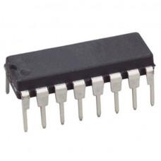
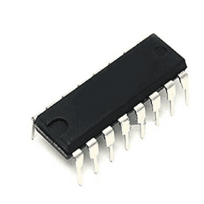
CD4504 - Hex Voltage-Level Shifter IC The CD4504 hex voltage level shifter IC consists of six circuits that shift input signals from the V CC logic level to the V DD logic level. To shift TTL signals to CMOS logic levels, the SELECT input is at the V CC HIGH logic state. When the SELECT input is in a LOW logic state, each circuit translates signals from one CMOS level to another. The CD4504 types are supplied in 16-lead hermetic dual-in-line ceramic packages (F3A suffix), 16-lead dual-in-line plastic packages (E suffix), 16-lead small-outline packages (M, M96, and MT suffixes), and 16-lead thin shrink small-outline packages (PW and PWR suffixes). Pinout: Pin No Pin Name Description 1 VCC Collector supply voltage 2 AOUT output of level shifter A 3 AIN input of level shifter A 4 BOUT output of level shifter B 5 BIN input of level shifter B 6 COUT output of level shifter C 7 CIN input of level shifter C 8 VSS source supply 9 DIN input of level shifter D 10 DOUT output of level shifter D 11 EIN input of level shifter E 12 EOUT output of level shifter E 13 SELECT select pin 14 FIN input of level shifter F 15 FOUT output of level shifter F 16 VDD Drain supply
- Independence of power-supply sequence considerations – VCC can exceed VDD; input signals can exceed both VCC and VDD
- Up and down level-shifting capability
- Shiftable input threshold for either CMOS or TTL compatibility
- Standardized symmetrical output characteristics
- 100% tested for quiescent current @ 20 V
- Maximum input current of 1 µA at 18 V over full package-temperature range; 100 nA at 18 V and 25°C
- 5V, 10 V, and 15 V parametric ratings
- Meets all requirements of JEDEC Standard No. 13B, “Standard Specifications for Description of ’B’ Series CMOS Devices”
- Part number CD4504
- Technology Family CD4000
- Bits (#) 6
- Voltage (Nom) (V) 5
- F @ nom voltage (Max) (MHz) 50
- ICC @ nom voltage (Max) (mA) 0.001
- IOL (Max) (mA) 6.8
- IOH (Max) (mA) -6.8
- Schmitt trigger No
- tpd @ nom Voltage (Max) (ns) 2.9


