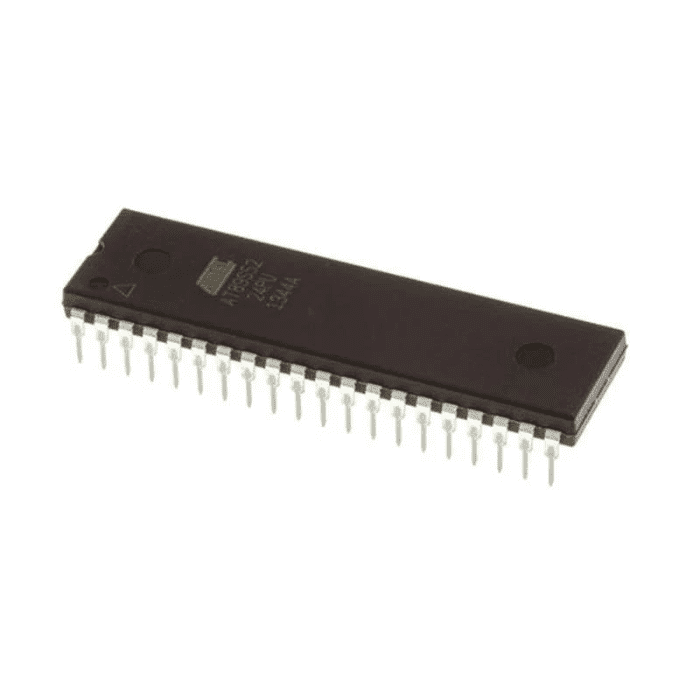
Atmel 89S52
Delivery & Pickup Options
This item is not available right now. Please check back later or contact us for availability.
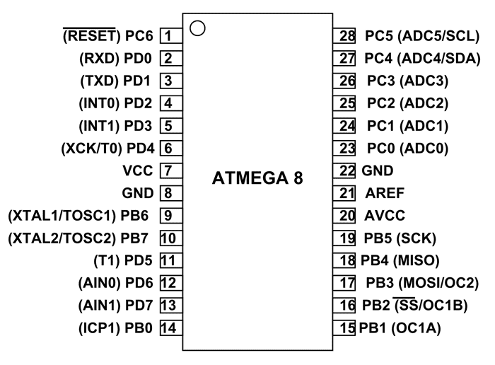
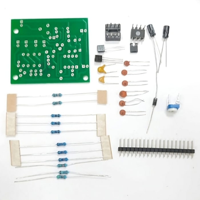
Atmel 89S52 The Atmel AT89S52 is a low-power, high-performance CMOS 8-bit microcontroller with 8K bytes of in-system programmable Flash memory. The device is manufactured using Atmel’s high-density nonvolatile memory technology and is compatible with the industry-standard 80C51 instruction set and pin out. The on-chip Flash allows the program memory to be reprogrammed in-system or by a conventional nonvolatile memory programmer. By combining a versatile 8-bit CPU with in-system programmable Flash on a monolithic chip, the Atmel AT89S52 is a powerful micro controller which provides a highly-flexible and cost-effective solution to many embedded control applications. The AT89S52 provides the following standard features like 8K bytes of Flash, 256 bytes of RAM, 32 I/O lines, Watchdog timer, two data pointers, three 16-bit timer/counters, a six-vector two-level interrupt architecture, a full duplex serial port, on-chip oscillator, and clock circuitry. In addition, the AT89S52 is designed with static logic for operation down to zero frequency and supports two software selectable power saving modes. The Idle Mode stops the CPU while allowing the RAM, timer/counters, serial port, and interrupt system to continue functioning. Pinout: Pinout Of Atmel 89S52 1 P1.0 (T2) Timer/Counter or 0th GPIO pin of PORT 1 2 P1.1 (T2.EX) Timer/Counter/External Counter or 1st GPIO pin of PORT 1 3 P1.2 2nd GPIO pin of PORT 1 4 P1.3 3rd GPIO pin of PORT 1 5 P1.4 4th GPIO pin of PORT 1 6 P1.5 (MOSI) MOSI for in System Programming or 5th GPIO pin of PORT 1 7 P1.6 (MISO) MISO for in System Programming or 6th GPIO pin of PORT 1 8 P1.7 (SCK) SCK for in System Programming or 7th GPIO pin of PORT 1 9 RST Making this pin high will reset the Microcontroller 10 P3.0 (RXD) RXD Serial Input or 0th GPIO pin of PORT 3 11 P3.1 (TXD) TXD Serial Output or 1st GPIO pin of PORT 3 12 P3.2 (INT0’) External Interrupt 0 or 2nd GPIO pin of PORT 3 13 P3.3 (INT1’) External Interrupt 1 or 3rd GPIO pin of PORT 3 14 P3.4 (T0) Timer 0 or 4th GPIO pin of PORT 3 15 P3.5 (T1) Timer 1 or 5th GPIO pin of PORT 3 16 P3.6 (WR’) Memory Write or 6th GPIO pin of PORT 3 17 P3.7 (RD’) Memory Read or 7th GPIO pin of PORT 3 18 XTAL2 External Oscillator Output 19 XTAL1 External Oscillator Input 20 GND Ground pin of MCU 21 P2.0(A8) 0th GPIO pin of PORT 2 22 P2.1 (A9) 1st GPIO pin of PORT 2 23 P2.2 (A10) 2nd GPIO pin of PORT 2 24 P2.3 (A11) 3rd GPIO pin of PORT 2 25 P2.4 (A12) 4th GPIO pin of PORT 2 26 P2.5 (A13) 5th GPIO pin of PORT 2 27 P2.6 (A14) 6th GPIO pin of PORT 2 28 P2.7 (A15) 7th GPIO pin of PORT 2 29 PSEN’ Program store Enable used to read external program memory 30 ALE / PROG’ Address Latch Enable / Program Pulse Input 31 EA’ / VPP External Access Enable / Programming enable Voltage 32 P0.7 (AD7) Address / Data pin 7 or 7th GPIO pin of PORT 0 33 P0.6 (AD6) Address / Data pin 6 or 6th GPIO pin of PORT 0 34 P0.5 (AD5) Address / Data pin 5 or 5th GPIO pin of PORT 0 35 P0.4 (AD4) Address / Data pin 4 or 4th GPIO pin of PORT 0 36 P0.3 (AD3) Address / Data pin 3 or 3rd GPIO pin of PORT 0 37 P0.2 (AD2) Address / Data pin 2 or 2nd GPIO pin of PORT 0 38 P0.1 (AD1) Address / Data pin 1 or 1st GPIO pin of PORT 0 39 P0.0 (AD0) Address / Data pin 0 or 0th GPIO pin of PORT 0 40 VCC Positive pin of MCU (+5V) Applications: Home automation Industrial automation Robotics Automotive Medical devices Communication devices
- Compatible with MCS-51 Products
- 8K Bytes of In-System Reprogrammable Flash Memory
- Fully Static Operation: 0 Hz to 24 MHz
- Three-level Program Memory Lock
- 256 x 8-bit Internal RAM
- 32 Programmable I/O Lines
- Three 16-bit Timer/Counters
- Eight Interrupt Sources
- Programmable Serial Channel
- Low-power Idle and Power-down Modes
- 40-pin DIP
- Programmable (ISP) Flash Memory 8K Bytes
- Endurance 1000 Write/Erase Cycles
- Operating Range 4.0V to 5.5V
- Fully Static Operation 0 Hz to 33 MHz
- Internal RAM 256 x 8-bit
- Programmable I/O Lines 32
- Dimensions 40x15x4mm
- Weight 2g