

Sort by

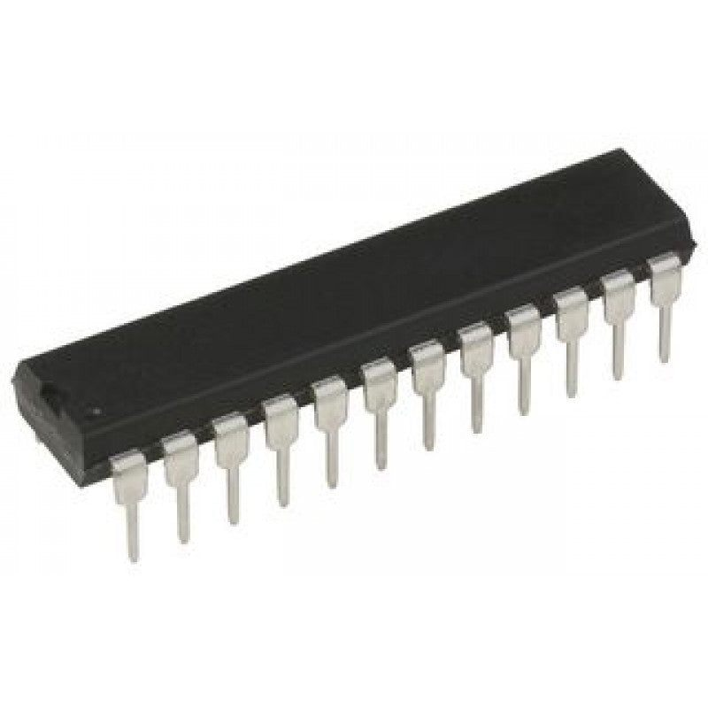
CD4034 - 8-Stage Bidirectiona…
CD4034 - 8-Stage Bidirectional Bus Register IC
The CD4034 Register
IC
is a static eight-stage parallel-or serial-input parallel-output register. It can be used to:
1) Bi-directionally transfer parallel information between two buses, 2) convert serial data to parallel form and direct the parallel data to either of two buses, 3) store (recirculate) parallel data, or 4) accept parallel data from either of two buses and convert that data to serial form. Input that controls the operations includes a single-phase CLOCK (CL), A-DATA ENABLE (AE), ASYNCHRONOUS/SYNCHRONOUS (A/S), A-BUS-TO-B-BUS/B-BUS-TO-A-BUS (A/B), and PARALLEL/SERIAL (P/S).
Data inputs include 16 bidirectional parallel data lines of which the eight A data lines are inputs (3-state outputs) and the B data lines are outputs (inputs) depending on the signal level on the A/B input. In addition, input for SERIAL DATA is also provided.
All register stages are D-type master-slave flip-flops with separate master and slave clock inputs generated internally to allow synchronous or asynchronous data transfer from master to slave. Isolation from external noise and the effects of loading is provided by output buffering.
Register expansion can be accomplished by simply cascading CD4034 packages.
The CD4034 types are supplied in 24-lead hermetic dual-in-line ceramic packages (F3A suffix), 24-lead dual-in-line plastic packages (E suffix), 24-lead small-outline packages (M, M96, and NSR suffixes), and 24-lead thin shrink small-outline packages (PW and PWR suffixes).
Pinout:
Pinout of CD4034 - 8-Stage Bidirectional Bus Register IC
Applications:
Parallel Input/Parallel Output, Serial Input/Parallel Output, Serial Input/Serial Output Register
Shift right/shift-left register
Shift right/shift left with parallel loading
Address register
Buffer register
Bus system register with enable parallel lines at bus side
Double bus register system
Up-Down Johnson or ring counter
Pseudo-random code generators
Sample and hold register (storage, counting, display)
Frequency and phase comparator
₹109,04
MRP. ₹197,40
Incl. GST (No Hidden Charges)
Incl. GST (No Hidden Charges)
CD4034 - 8-Stage Bidirectional Bus Register IC (Original)
CD4034 - 8-Stage Bidirectional Bus Register IC The CD4034 Register IC is a static eight-stage parallel-or serial-input parallel-output register. It can be used to: 1) Bi-directionally transfer parallel information between …
As low as
₹109,04
₹109,04
MRP. ₹197,40
Incl. GST (No Hidden Charges)
CD4040 - 12-Stage Ripple Carr…
CD4040 - 12-Stage Ripple Carry Binary Counter IC
The
CD4x Series
CD4040 is a ripple-carry binary counter that features 12 stages, push-pull type, and balanced outputs, with standard speed (TPD > 50ns). All counter stages are master-slave flip-flops. Supports wide input voltage ranges from 3V to 18V. The maximum input current at 18V is 1 uA whereas 100 nA at 18V and 25°C.
All counter stages are master-slave flip-flops. The state of a counter advances one count on the negative transition of each input pulse; a high level on the RESET line resets the counter to its all-zeros state. Schmitt's trigger action on the input-pulse line permits unlimited rise and fall times. All inputs and outputs are buffered. 16 Pin DIP is available in a hermetic dual-in-line ceramic package.
We also have a
CD4020
with similar features. The differences are CD4020 is a 14 Stage binary counter whereas CD4040 is a 12 Stage binary counter and there is a difference between the pin layout.
check out :
CD4518 - Dual BCD Up Counter IC (Original)
Pinout:
Pinout of CD4040 IC
Applications:
Control Counters
Timers
Frequency Dividers
Time-Delay Circuits
₹31,15
MRP. ₹47,60
Incl. GST (No Hidden Charges)
Incl. GST (No Hidden Charges)
CD4040 - 12-Stage Ripple Carry Binary Counter IC
CD4040 - 12-Stage Ripple Carry Binary Counter IC The CD4x Series CD4040 is a ripple-carry binary counter that features 12 stages, push-pull type, and balanced outputs, with standard speed (TPD …
As low as
₹31,15
₹31,15
MRP. ₹47,60
Incl. GST (No Hidden Charges)
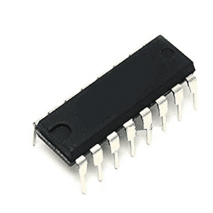
CD4046 - Micropower Phase Loc…
CD4046 - Micropower Phase Locked Loop IC
CD4046 CMOS Micropower Phase-Locked Loop (PLL) IC consists of a low-power, linear voltage-controlled oscillator (VCO) and two different phase comparators having a common signal-input amplifier and a common comparator input. A 5.2-V Zener diode is provided for supply regulation if necessary.
The
CD series
CD4046 types are supplied in 16-lead hermetic dual-in-line ceramic packages (F3A suffix), 16-lead dual-in-line plastic packages (E suffix), 16-lead small-outline packages (NSR suffix), and 16-lead thin shrink small-outline packages (PW and PWR suffixes).
check out :
Dual JK Flip Flop IC - CD4027
Pinout:
Pinout of CD4046 IC
Applications:
FM demodulator and modulator
Frequency synthesis and multiplication
Frequency discriminator
Data synchronization
Voltage-to-frequency conversion
Tone decoding
FSK - Modems
Signal conditioning
₹30,04
MRP. ₹50,40
Incl. GST (No Hidden Charges)
Incl. GST (No Hidden Charges)
CD4046 - Micropower Phase Locked Loop IC
CD4046 - Micropower Phase Locked Loop IC CD4046 CMOS Micropower Phase-Locked Loop (PLL) IC consists of a low-power, linear voltage-controlled oscillator (VCO) and two different phase comparators having a common …
As low as
₹30,04
₹30,04
MRP. ₹50,40
Incl. GST (No Hidden Charges)
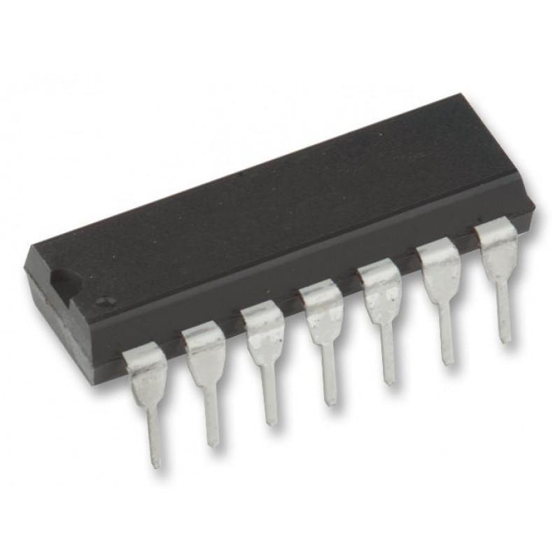
CD4047 - Astable/Monostable M…
CD4047 - Astable/Monostable Multivibrator IC
CD4047
IC
consists of a gateable astable multivibrator with logic techniques incorporated to permit positive or negative edge-triggered monostable multivibrator action with retriggering and external counting options.
Inputs include +TRIGGER, -TRIGGER, ASTABLE, ASTABLE\, RETRIGGER, and EXTERNAL RESET. Buffered outputs are Q\, Q an OSCILLATOR. In all modes of operation, an external capacitor must be connected between C-Timing and RC-Common terminal, and an external resistor must be connected between the R-Timing and RC-Common terminals.
Astable operation is enabled by a high level on the STABLE input or a low level on the ASTABLE\ input, or both. The period of the square wave at the Q and Q\ Outputs in this mode of operation is a function of the external components employed. "True" input pulses on the ASTABLE input or "Complement" pulses on the ASTABLE\ input allow the circuit to be used as a gateable multivibrator. The OSCILLATOR output period will be half of the Q terminal output in the astable mode. However, a 50% duty cycle is not guaranteed at this output.
The CD4047 triggers in the monostable mode when a positive-going edge occurs on the +TRIGGER-input while the -TRIGGER is held low. Input pulses may be of any duration relative to the output pulse.
The CD4047-Series types are supplied in 14-lead hermetic dual-in-line ceramic packages (F3A suffix), 14-lead dual-in-line plastic packages (E suffix), 14-lead small-outline packages (M, MT, M96, and NSR suffixes), and 14-lead thin shrink small-outline packages (PW and PWR suffixes).
check out :
CD4094 - 8-Stage Shift and Store Bus Register IC
Pinout:
Pinout of CD4047 IC
Applications:
Digital equipment where low-power dissipation and/or high noise immunity are primary design requirements:
Envelope detection
Frequency multiplication
Frequency division
Frequency discriminators
Timing circuits
Time-delay applications
₹24,49
Incl. GST (No Hidden Charges)
Out of Stock
MRP. ₹49,00
Incl. GST (No Hidden Charges)
CD4047 - Astable/Monostable Multivibrator IC
CD4047 - Astable/Monostable Multivibrator IC CD4047 IC consists of a gateable astable multivibrator with logic techniques incorporated to permit positive or negative edge-triggered monostable multivibrator action with retriggering and external …
As low as
₹24,49
₹24,49
MRP. ₹49,00
Incl. GST (No Hidden Charges)
Out of Stock
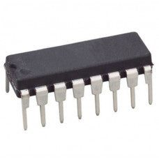
CD4049 - Hex Inverting Buffer…
CD4049 - Hex Inverting Buffer/Converter IC
The
CD4x Series
CD4049 hex buffers are monolithic complementary MOS (CMOS) integrated circuits constructed with N- and P-channel enhancement mode transistors. These devices feature logic-level conversion using only one supply voltage (VDD).
The input signal level can exceed the VDD supply voltage when these devices are used for logic-level conversions. These devices are intended for use as hex buffers, CMOS to DTL/TTL converters, or as CMOS current drivers, and at VDD=5.0V, they can drive directly two DTL/TTL loads over the full operating temperature range.
check out :
CD4504 - Hex Voltage Level Shifter IC
Pinout:
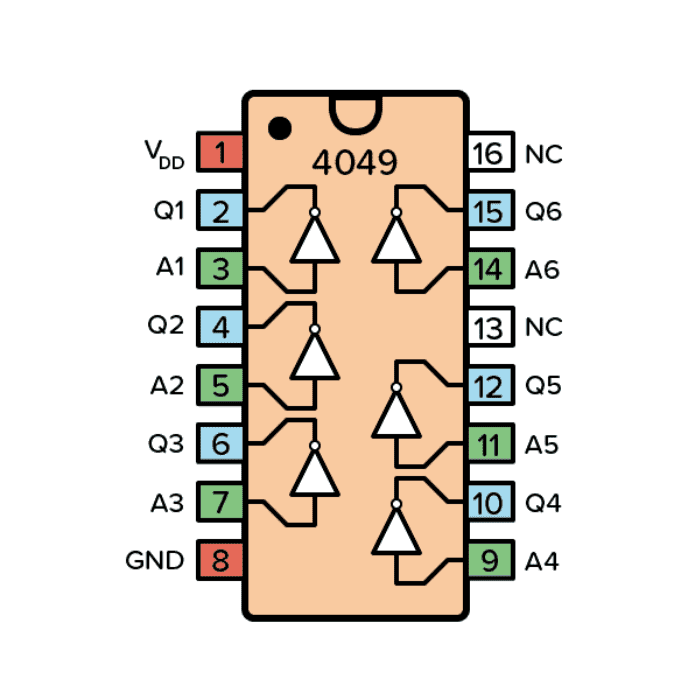
Pinout Of CD4049 IC
Pin Name
Pin #
Type
Description
VDD
1
Power
Supply Voltage (+3 to +15V)
GND
8
Power
Ground (0V)
Q1-Q6
2, 4, 6, 10, 12, 15
Input
Inputs to the inverters
A1-A6
3, 5, 7, 9, 11, 14
Output
Outputs from the inverters
NC
13, 16
–
Not Connected
Applications:
CMOS hex inverter/buffer
CMOS to DTL/TTL hex converter
CMOS current "sink" or "source" driver
CMOS high-to-low logic level converter
₹22,25
MRP. ₹47,60
Incl. GST (No Hidden Charges)
Incl. GST (No Hidden Charges)

CD4049 - Hex Inverting Buffer/Converter IC
CD4049 - Hex Inverting Buffer/Converter IC The CD4x Series CD4049 hex buffers are monolithic complementary MOS (CMOS) integrated circuits constructed with N- and P-channel enhancement mode transistors. These devices feature …
As low as
₹22,25
₹22,25
MRP. ₹47,60
Incl. GST (No Hidden Charges)
CD4050 - Hex Non-Inverting Bu…
CD4050 - Hex Non-Inverting Buffer IC
The CD4050 hex buffers
IC
are monolithic complementary MOS (CMOS) integrated circuits constructed with N- and P-channel enhancement mode transistors. These devices feature logic-level conversion using only one supply voltage (VDD).
The input signal high level (VIH) can exceed the VDD supply voltage when these devices are used for logic-level conversions. These devices are intended for use as hex buffers IC, CMOS to DTL/ TTL converters, or as CMOS current drivers, and at VDD = 5.0V, they can drive directly two DTL/TTL loads over the full operating temperature range.
check out :
CD4069 - Hex Inverter IC
Pinout:
Pinout of CD4050 - Hex Non-Inverting Buffer IC
Applications:
CMOS hex inverter/buffer.
CMOS to DTL/TTL hex converter.
CMOS current “sink” or “source” driver.
CMOS HIGH-to-LOW logic level converter.
₹25,59
MRP. ₹40,60
Incl. GST (No Hidden Charges)
Incl. GST (No Hidden Charges)

CD4050 - Hex Non-Inverting Buffer IC
CD4050 - Hex Non-Inverting Buffer IC The CD4050 hex buffers IC are monolithic complementary MOS (CMOS) integrated circuits constructed with N- and P-channel enhancement mode transistors. These devices feature logic-level …
As low as
₹25,59
₹25,59
MRP. ₹40,60
Incl. GST (No Hidden Charges)
CD4051 - Single 8-channel Mul…
CD4051 - Single 8-channel Multiplexer/Demultiplexer IC
The CD4051 analog multiplexers and demultiplexers
IC
are digitally-controlled analog switches having low ON impedance and very low OFF leakage current. These multiplexer circuits dissipate extremely low quiescent power over the full V
DD
– V
SS
and V
DD
– V
EE
supply-voltage ranges, independent of the logic state of the control signals.
Pinout:
Pinout of CD4051 Multiplexer/Demultiplexer IC
₹23,36
MRP. ₹47,60
Incl. GST (No Hidden Charges)
Incl. GST (No Hidden Charges)
CD4051 - Single 8-channel Multiplexer/Demultiplexer IC
CD4051 - Single 8-channel Multiplexer/Demultiplexer IC The CD4051 analog multiplexers and demultiplexers IC are digitally-controlled analog switches having low ON impedance and very low OFF leakage current. These multiplexer circuits …
As low as
₹23,36
₹23,36
MRP. ₹47,60
Incl. GST (No Hidden Charges)
CD4052 - Differential 4-chann…
CD4052 - Differential 4-channel Multiplexer/Demultiplexer IC
The CD4052 analog multiplexers/demultiplexers
IC
are digitally controlled analog switches having low “ON” impedance and very low “OFF” leakage currents. Control of analog signals up to 15Vp-p can be achieved by digital signal amplitudes of 3?15V. For example, if VDD = 5V, VSS = 0V and VEE = ?5V, analog signals from ?5V to +5V can be controlled by digital inputs of 0?5V.
The multiplexer circuits dissipate extremely low quiescent power over the full VDD?VSS and VDD?VEE supply voltage ranges, independent of the logic state of the control signals. When a logical “1” is present at the inhibit input terminal all channels are “OFF”. CD4052 is a differential 4-channel multiplexer having two binary control inputs, A and B, and an inhibit input. The two binary input signals select 1 or 4 pairs of channels to be turned on and connect the differential analog inputs to the differential outputs.
Pinout:
Pinout of CD4052 - Differential 4-channel Multiplexer/Demultiplexer IC
Pin Number
Pin Name
Description
16
Vdd
Positive power input, maximum 20V
7
Vee
Negative power rail, normally connected to ground.
8
Vss (Ground)
Connected to ground of the circuit
6
INH
Enable pin – Must be pulled to ground for normal operation
9,10
A,B
Channel Select pins
1,12
Y0,X0
Channel 0 Input / Output
5,14
Y1,X1
Channel 1 Input / Output
2,15
Y2,X2
Channel 2 Input / Output
4,11
Y3,X3
Channel 3 Input / Output
3,13
Y,X
Common Output / Input
₹18,92
MRP. ₹40,60
Incl. GST (No Hidden Charges)
Incl. GST (No Hidden Charges)

CD4052 - Differential 4-channel Multiplexer/Demultiplexer IC
CD4052 - Differential 4-channel Multiplexer/Demultiplexer IC The CD4052 analog multiplexers/demultiplexers IC are digitally controlled analog switches having low “ON” impedance and very low “OFF” leakage currents. Control of analog signals …
As low as
₹18,92
₹18,92
MRP. ₹40,60
Incl. GST (No Hidden Charges)
CD4053 - Triple 2-channel Mul…
CD4053 - Triple 2-channel Multiplexer/Demultiplexer IC
The CD4053 IC analog multiplexers demultiplexers are digitally controlled analog switches having low “ON” impedance and very low “OFF” leakage currents. Control of analog signals up to 15Vp-p can be achieved by digital signal amplitudes of 3?15V. For example, if VDD = 5V, VSS = 0V and VEE = ?5V, analog signals from ?5V to +5V can be controlled by digital inputs of 0?5V. The multiplexer circuits dissipate extremely low quiescent power over the full VDD?VSS and VDD?VEE supply voltage ranges, independent of the logic state of the control signals. When a logical “1” is present at the inhibit input terminal all channels are “OFF”.
The
CD4x Series
CD4053 Integrated Circuits is a triple 2-channel multiplexer having three separate digital control inputs, A, B, and C, and an inhibit input. Each control input selects one of a pair of channels that are connected in a single-pole double-throw configuration.
Pinout:
Pin No
Pin Name
Description
1
Y1
Y1 Switch Input/Output
2
Y0
Y0 Switch Input/Output
3
Z1
Z1 Switch Input/Output
4
Z
Input/Output Z
5
Z0
Z0 Switch Input/Output
6
INH
Inhibit Input
7
VEE
Emitter supply
8
VSS
Source Supply
9
C
Digital Control Input C
10
B
Digital Control Input B
11
A
Digital Control Input A
12
X0
X0 Switch Input/Output
13
X1
X1 Switch Input/Outputs
14
X
Input/Output X
15
Y
Input/Output Y
16
VDD
Drain supply
Applications:
Analog multiplexing and demultiplexing
Digital multiplexing and demultiplexing
Signal gating
₹24,49
MRP. ₹47,60
Incl. GST (No Hidden Charges)
Incl. GST (No Hidden Charges)
CD4053 - Triple 2-channel Multiplexer/Demultiplexer IC
CD4053 - Triple 2-channel Multiplexer/Demultiplexer IC The CD4053 IC analog multiplexers demultiplexers are digitally controlled analog switches having low “ON” impedance and very low “OFF” leakage currents. Control of analog …
As low as
₹24,49
₹24,49
MRP. ₹47,60
Incl. GST (No Hidden Charges)
CD4059 - Programmable Divide-…
CD4059 - Programmable Divide-by-N Counter IC
The
CD4x Series
CD4059 standard "A" Series types are divide-by-N down-counters that can be programmed to divide an input frequency by any number "N" from 3 to 15,999. The output signal is a pulse one clock-cycle wide occurring at a rate equal to the input frequency divided by N. This single output has TTL drive capability. The down-counter is preset by means of 16 jam inputs.
The three Mode-Select Inputs Ka, Kb, and Kc determine the modulus ("divide-by" number) of the first and last counting sections. Every time the first (fastest) counting section goes through one cycle, it reduces by 1 the number that has been preset (jammed) into the three decades of the intermediate counting section and into the last counting section, which consists of flip-flops that are not needed for operating the first counting section.
For example, in the 2 modes, only one flip-flop is needed in the first counting section. Therefore the last counting section has three flip-flops that can be preset to a maximum count of seven with a place value of thousands. If 10 is desired for the first section, Ka is set to 1, Kb to 1, and Kc to 0. Jam Inputs J1, J2, J3, and J4 are used to preset the first counting section and there is no last counting section. The intermediate counting section consists of three cascaded BCD decade (10) counters presettable by means of Jam Inputs J5 through J16.
This device is particularly advantageous in communication digital frequency synthesis (VHF, UHF, FM, AM, etc.) where programmable divide-by-"N" counters are an integral part of the synthesizer phase-locked-loop sub-system. The CD4059 can also be used to perform the synthesizer "Fixed Divide-by-R" counting function. It is also useful in general-purpose counters for instrumentation functions such as totalizers, production counters, and "time-out" timers.
The CD4059B-series types are supplied in 24-lead dual-in-line plastic packages (E suffix), and 24-lead small-outline packages (M and M96 suffixes).
Pinout:
Pinout of CD4059 IC
Applications:
Communications digital frequency synthesizers: VHF, UHF, FM, AM, etc.
Fixed or programmable frequency division
"Time out" timer for consumer-application industrial controls
Companion Application Note, ICAN-6374, "Application of the CMOS CD4059A Programmable Divide-by-N Counter in FM and Citizens Band Transceiver Digital Tuners"
₹180,27
Incl. GST (No Hidden Charges)
Out of Stock
MRP. ₹330,40
Incl. GST (No Hidden Charges)
CD4059 - Programmable Divide-by-N Counter IC
CD4059 - Programmable Divide-by-N Counter IC The CD4x Series CD4059 standard "A" Series types are divide-by-N down-counters that can be programmed to divide an input frequency by any number "N" …
As low as
₹180,27
₹180,27
MRP. ₹330,40
Incl. GST (No Hidden Charges)
Out of Stock
