

Sort by
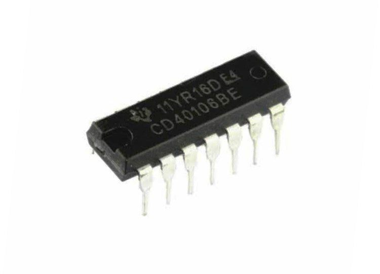
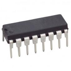
CD40106 - Hex Schmitt Trigger…
CD40106 - Hex Schmitt Trigger Inverter IC
The CD40106
IC
consists of six Schmitt-Trigger inputs. Each circuit functions as an inverter with Schmitt-Trigger input. The trigger switches at different points for positive- and negative-going signals. The difference between the positive-going voltage (VP) and the negative-going voltage (VN) is defined as hysteresis voltage (VH).
A Schmitt trigger input means that the threshold voltage for going from a HIGH to a LOW input is different from the threshold for going from LOW to HIGH.
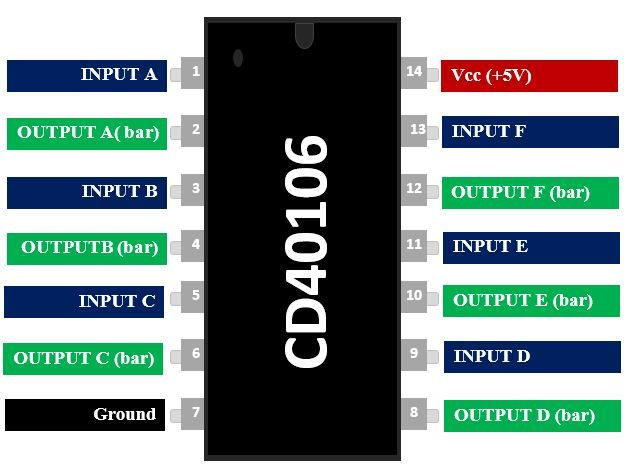
CD40106
Pinout Configuration:
Pin Number
Pin Name
Description
1,3,5,11,13,15
Schmitt Input Pins
Input pins of the Schmitt trigger
2,4,6,10,12,14
Schmitt Inverted Output Pins
Output pins of the Schmitt trigger
7
Ground
Connected to the ground of the system
14
Vcc (+5V)
Resets all outputs as low. Must be held high for normal operation
Applications of CD40106:
Noise removing circuits
Debouncing circuits
Hysteresis controller
Dead band filter
₹23,36
MRP. ₹47,60
Incl. GST (No Hidden Charges)
Incl. GST (No Hidden Charges)
CD40106 - Hex Schmitt Trigger Inverter IC
CD40106 - Hex Schmitt Trigger Inverter IC The CD40106 IC consists of six Schmitt-Trigger inputs. Each circuit functions as an inverter with Schmitt-Trigger input. The trigger switches at different points …
As low as
₹23,36
₹23,36
MRP. ₹47,60
Incl. GST (No Hidden Charges)
CD4011 - Quad 2-Input NAND Ga…
CD4011 - Quad 2-Input NAND Gate IC
The
CD4011 is a quad package 2-Input NAND gate
IC
(Integrated Circuits). That is, it has four NAND gates inside a single package and each gate has two input lines and one output line. All the inputs and outputs are buffered and this improves transfer characteristics by providing a very high gain.
The CD4011 IC
operates at 5V, 10V, 15V, and even 20V. When operating at 5V the maximum low-level input voltage is 0.5 and the minimum high-level input voltage is 4.5. All four gates share the same power rail but can operate independently.
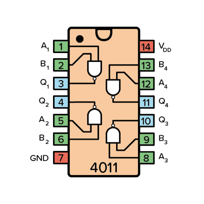
Pinout:
Pinout Of CD4011 IC
₹22,25
MRP. ₹47,60
Incl. GST (No Hidden Charges)
Incl. GST (No Hidden Charges)
CD4011 - Quad 2-Input NAND Gate IC
CD4011 - Quad 2-Input NAND Gate IC The CD4011 is a quad package 2-Input NAND gate IC (Integrated Circuits). That is, it has four NAND gates inside a single package …
As low as
₹22,25
₹22,25
MRP. ₹47,60
Incl. GST (No Hidden Charges)

CD4013 - Dual D Type Flip-Flo…
CD4013 - Dual D Type Flip-Flop IC
The CD4013 designed as a CMOS logic chip IC belongs to the CD4XXX IC series. The CD4013 device comprises two identical, independent data-type flip-flops. Each flip-flop comes with independent data, set, reset, and clock inputs, and Q and Q’ outputs. These devices are commonly used for shift register applications, and, by connecting Q output to the data input, for counter and toggle applications. The logic level present at the D input is transmitted to the Q output during the positive-going transition of the clock pulse. Moreover, the Setting or resetting of IC is independent of the clock and accomplished by a high level on the set or reset line, respectively. The CD4013B is manufactured in 14-pin dual-inline plastic packages (E suffix), 14-pin small-outline packages (M, MT, M96, and NSR suffixes), and 14-pin thin shrink small-outline packages (PW and PWR suffixes).
A D-type Latch/flip-flop is designed as a
clocked latch that has two stable states. A D-type latch operates with a delay in input by one clock cycle. Thus, by cascading many D-type flip-flops delay circuits
are often
created, which are
utilized in
many applications
like
in digital television systems. A D-type flip-flop is additionally
mentioned
as a D flip-flop or a delay flip-flop. The D flip-flop is an edge-triggered device that transfers
input files
to Q on a clock rising or falling edge. Data Latches are level sensitive devices
like
the data
latch
and therefore the
transparent latch.
Applications
Power Delivery
Grid Infrastructure
Medical, Healthcare, and Fitness
Body Electronics and Lighting
Building Automation
Telecom Infrastructure
Test and Measurement
₹16,69
MRP. ₹26,60
Incl. GST (No Hidden Charges)
Incl. GST (No Hidden Charges)
CD4013 - Dual D Type Flip-Flop IC
CD4013 - Dual D Type Flip-Flop IC The CD4013 designed as a CMOS logic chip IC belongs to the CD4XXX IC series. The CD4013 device comprises two identical, independent data-type …
As low as
₹16,69
₹16,69
MRP. ₹26,60
Incl. GST (No Hidden Charges)
CD4015 - Dual 4-Stage Shift R…
CD4015 - Dual 4-Stage Shift Register IC
The CD4015
IC
consists of two identical, independent, 4-stage serial-input/parallel-output registers. Each register has independent CLOCK and RESET inputs as well as a single serial DATA input. “Q” outputs are available from each of the four stages on both registers. All register stages are D-type, master-slave flip-flops. The logic level present at the DATA input is transferred into the first register stage and shifted over one stage at each positive-going clock transition. Resetting of all stages is accomplished by a high level on the reset line. Register expansion to 8 stages using one CD4015 package, or to more than 8 stages using additional CD4015’s is possible.
The CD4015-series types are supplied in 16-lead hermetic dual-in-line ceramic packages (F3A suffix), 16-lead dual-in-line plastic package (E suffix), 16-lead small-outline packages (M, M96, MT, and NSR suffixes), and 16-lead thin shrink small-outline packages (PW and PWR suffixes).
check out :
CD4034 - 8-Stage Bidirectional Bus Register IC (Original)
Pinout:
Pinout Of CD4015 - Dual 4-Stage Shift Register IC
Pin Name
Pin #
Type
Description
VDD
16
Power
Supply Voltage (+3 to +15V)
GND
8
Power
Ground (0V)
D
A
7
Input
Data pin for register A
CLK
A
9
Input
Clock pulse for register A
RST
A
6
Input
Reset pin for register A
Q
A0
,Q
A1
,Q
A2
,Q
A3
5,4,3,10
Output
4-bit output for register A
D
B
15
Input
Data pin for register B
CLK
B
1
Input
Clock pulse for register B
RST
B
14
Input
Reset pin for register B
Q
B0
,Q
B1
,Q
B2
,Q
B3
11,12,13, 2
Output
4-bit output for register B
Applications:
Serial-input/parallel-output data queueing
Serial to parallel data conversion
General-purpose register
₹25,59
MRP. ₹50,40
Incl. GST (No Hidden Charges)
Incl. GST (No Hidden Charges)

CD4015 - Dual 4-Stage Shift Register IC
CD4015 - Dual 4-Stage Shift Register IC The CD4015 IC consists of two identical, independent, 4-stage serial-input/parallel-output registers. Each register has independent CLOCK and RESET inputs as well as a …
As low as
₹25,59
₹25,59
MRP. ₹50,40
Incl. GST (No Hidden Charges)
CD4016 - Quad Bilateral Switc…
CD4016 - Quad Bilateral Switch IC
The
CD4x Series
CD4016 is a quad bilateral switch intended for the transmission or multiplexing of analog or digital signals. It is pin-for-pin compatible with CD4066B.
The CD4016 is a CMOS IC with four analog switches, which can be controlled individually using a control pin. The signal can flow in either direction between the two pins of each switch.
Each switch has an enable pin (A) and two input/output pins (X and Y). When the enable pin is set to HIGH, current can flow between X and Y in either direction. However, when enable is LOW, no current can flow between the pins. Just like a switch.
Pinout:
Pinout of CD4016 IC
Pin Name
Pin #
Type
Description
VDD
14
Power
Supply Voltage (+3 to +15V)
GND
7
Power
Ground (0V)
A1-A4
5,6,12,13
Input
Enable pins for the four bilateral switches
X1-X4
1,3,9,11
Input/Output
Pin X for each switch
Y1-Y4
2,4,8,10
Input/Output
Pin Y for each switch
₹24,49
MRP. ₹47,60
Incl. GST (No Hidden Charges)
Incl. GST (No Hidden Charges)
CD4016 - Quad Bilateral Switch IC
CD4016 - Quad Bilateral Switch IC The CD4x Series CD4016 is a quad bilateral switch intended for the transmission or multiplexing of analog or digital signals. It is pin-for-pin compatible …
As low as
₹24,49
₹24,49
MRP. ₹47,60
Incl. GST (No Hidden Charges)
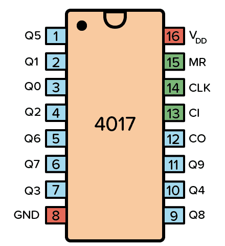
CD4017 - Decade Counter IC
CD4017 - Decade Counter IC
The CD4017
IC
is a
decade counter
that counts to ten. It has 10 outputs that represent the numbers 0 to 9. The counter increases with one for every rising clock pulse. After the counter has reached 9, it starts again from 0 with the next clock pulse.
This is a great chip for making running LEDs! See a circuit example further down.
check out :
Dual Complementary Pair with Inverter IC - CD4007
Pin Overview:
Pinout of CD4017 - Decade Counter IC
Pin Name
Pin #
Type
Description
VDD
16
Power
Supply Voltage (+3 to +15V)
GND
8
Power
Ground (0V)
Q0-Q9
1-7 and 9-11
Output
Qx is high when the counter is x
CO
12
Output
Carry Out. Goes high after ten clock pulses
CI
13
Input
Clock Inhibit. Ignores clock inputs
CLK
14
Input
Clock Input. Increases the counter with one
MR
15
Input
Resets the counter to 0
₹14,47
MRP. ₹25,20
Incl. GST (No Hidden Charges)
Incl. GST (No Hidden Charges)

CD4017 - Decade Counter IC
CD4017 - Decade Counter IC The CD4017 IC is a decade counter that counts to ten. It has 10 outputs that represent the numbers 0 to 9. The counter increases …
As low as
₹14,47
₹14,47
MRP. ₹25,20
Incl. GST (No Hidden Charges)
CD4028 - BCD to Decimal Decod…
CD4028 - BCD to Decimal Decoder IC
CD4028 IC is a BCD to decimal or binary to octal decoder consisting of 4 inputs and 10 output buffers. A BCD code is applied to the 4 inputs, A, B, C, and D. Thus resulting in a high level at the selected 1-of-10 decimal decoded outputs. Similarly, a 3-bit binary code applied to inputs A, B, and C is decoded into octal at outputs 0–7. A high-level signal at the D input inhibits octal decoding and causes outputs 0–7 to go LOW.
The
IC
is always available in a 16–pin hermetically sealed dual inline IC package (DIP), making it easy to interface with TTL, CMOS, and NMOS devices. The IC offers many features such as high noise immunity and low thermal dissipation. High drive capability is provided at all outputs to enhance dc and dynamic performance in high fan- ut applications. Meanwhile, all the inputs are protected against static discharge damage by diode clamps to V
DD
and V
SS
.
A BCD to Decimal Decoder is defined as a simple logic circuit that can translate a BCD (binary coded decimal) input into a decimal (0 – 9) output In any BCD to decimal decoder, the inverters are connected in pairs to make BCD input data available for decoding by the NAND gates. Full decoding of valid BCD input logic ensures that all outputs remain OFF for all invalid binary input conditions. Moreover, these decoders feature TTL inputs and high–performance NPN output transistors designed for use as indicator/relay drivers or as open–collector logic circuit drivers.
check out :
CD4514 - 4 Bit Latch/4-16 Line Decoder IC
Pinout:
Pinout of CD4028 IC
Application
Code conversion
Address decoding
Indicator-tube decoder
₹22,25
MRP. ₹47,60
Incl. GST (No Hidden Charges)
Incl. GST (No Hidden Charges)
CD4028 - BCD to Decimal Decoder IC
CD4028 - BCD to Decimal Decoder IC CD4028 IC is a BCD to decimal or binary to octal decoder consisting of 4 inputs and 10 output buffers. A BCD code …
As low as
₹22,25
₹22,25
MRP. ₹47,60
Incl. GST (No Hidden Charges)
CD4029 - Binary Decade Up-Dow…
CD4029 - Binary Decade Up-Down Counter IC
The CD4029 IC consists of a four-stage binary or BCD-decade up/ down counter with provisions for look-ahead carry in both counting modes. The inputs consist of a single CLOCK, CARRY-IN (CLOCK ENABLE), BINARY/DECADE, UP/DOWN, PRESET ENABLE, and four individual JAM signals. Q1, Q2, Q3, Q4, and a CARRY OUT signal are provided as outputs.
A high PRESET ENABLE signal allows information on the JAM INPUTS to preset the counter to any state asynchronously with the clock. A low on each JAM line, when the PRESET-ENABLE signal is high, resets the counter to its zero counts. The counter is advanced one count at the positive transition of the clock when the CARRY-IN and PRE-SET ENABLE signals are low. Advancement is inhibited when the CARRY-IN or PRESET ENABLE signals are high. The CARRY-OUT signal is normally high and goes low when the counter reaches its maximum count in the UP mode or the minimum count in the DOWN mode provided the CARRY-IN signal is low. The CARRY-IN signal in the low state can thus be considered a CLOCK ENABLE.
The CARRY-IN terminal must be connected to VSS when not in use. Binary counting is accomplished when the BINARY/DECADE input is high; the counter counts in the decade mode when the BINARY/DECADE input is low. The counter counts up when the UP/DOWN input is high, and down when the UP/DOWN input is low. Multiple packages can be connected in either a parallel clocking or a ripple-clocking arrangement as shown in Figure 17. Parallel clocking provides synchronous control and hence faster response from all counting outputs. Ripple-clocking allows for longer clock input rise and fall times. The
CD4x Series
CD4029 is supplied in these 16-lead outline packages: Braze Seal DIP H4X Frit Seal DIP H1F Ceramic Flatpack H6W.
Pinout:
Pinout of CD4029 IC
₹42,28
MRP. ₹61,60
Incl. GST (No Hidden Charges)
Incl. GST (No Hidden Charges)
CD4029 - Binary Decade Up-Down Counter IC
CD4029 - Binary Decade Up-Down Counter IC The CD4029 IC consists of a four-stage binary or BCD-decade up/ down counter with provisions for look-ahead carry in both counting modes. The …
As low as
₹42,28
₹42,28
MRP. ₹61,60
Incl. GST (No Hidden Charges)
CD4030 - Quad 2-Input Exclusi…
CD4030 - Quad 2-Input Exclusive OR (EXOR) Gate IC
The CD4030
IC
types consist of four independent Exclusive-OR gates. The CD4030 provides the system designer with a means for direct implementation of the Exclusive-OR function.
The CD4030 types are supplied in 14-lead hermetic dual-in-line ceramic packages (F3A suffix), 14-lead dual-in-line plastic packages (E suffix), 14-lead small-outline packages (M, MT, M96, and NSR suffixes), and 14-lead thin shrink small-outline packages (PW and PWR suffixes).
check out :
CD4519 - Quad AND/OR Select Gate IC (Original)
Pinout:
Pinout of CD4030 - Quad 2-Input Exclusive OR (EXOR) Gate IC
Applications:
Even and odd-parity generators and checkers
Logical comparators
Adders/subtractors
General logic functions
check out :
CD4081 - Quad 2 Input AND Gate IC
₹25,59
MRP. ₹50,40
Incl. GST (No Hidden Charges)
Incl. GST (No Hidden Charges)
CD4030 - Quad 2-Input Exclusive OR (EXOR) Gate IC
CD4030 - Quad 2-Input Exclusive OR (EXOR) Gate IC The CD4030 IC types consist of four independent Exclusive-OR gates. The CD4030 provides the system designer with a means for direct …
As low as
₹25,59
₹25,59
MRP. ₹50,40
Incl. GST (No Hidden Charges)
CD4033 - 5-Stage Johnson Deca…
CD4033 - 5-Stage Johnson Decade counter IC
The CD4033
IC
consists of a 5-stage Johnson decade counter IC and an output decoder that converts the Johnson code to a 7-segment decoded output for driving one stage in a numerical display.
These devices are particularly advantageous in display applications where low power dissipation and /or low package count are important.
Inputs common to both types are CLOCK, RESET, & CLOCK INHIBIT; common outputs are CARRY OUT and the seven decoded outputs (a, b, c, d, e, f, g). Signals peculiar to the CD4033 are RIPPLE-BLANKING INPUT AND LAMP TEST INPUT and a RIPPLE-BLANKING OUTPUT.
A high RESET signal clears the decade counter to its zero counts. The counter is advanced one count at the positive clock signal transition if the CLOCK INHIBIT signal is low. Counter advancement via the clock line is inhibited when the CLOCK INHIBIT signal is high. The CLOCK INHIBIT signal can be used as a negative-edge clock if the clock line is held high. Anti-lock gating is provided on the JOHNSON counter, thus assuring proper counting sequence. The CARRY-OUT (C
out
) signal completes one cycle every ten CLOCK INPUT cycles and is used to clock the succeeding decade directly in a multi-decade counting chain. The seven decoded outputs (a, b, c, d, e, f, g) illuminate the proper segments in a seven-segment display device used for representing the decimal numbers 0 to 9. The 7-segment outputs go high on selection in the CD4033.
The CD4033 series types are supplied in 16-lead dual-in-line plastic packages (E suffix), 16-lead small-outline packages (NSR suffix), and 16-lead thin shrink small-outline packages (PW and PWR suffixes).
Pinout:
Pinout of CD4033 - 5-Stage Johnson Decade counter IC
Pin 1 known as Clock in
– It receives clock signals, and at every positive clock counter advances one by one. You can provide a clock with the switch, 555 timer or the help of logic gates.
Pin 2 known as Clock inhibit
– CD4033 counter advances one by one by receiving a positive pulse at this time clock inhibit pin should be grounded. If it is connected to the supply then counter advancement will be inhibited means there will be no meaning of clock pulse.
Pin 3 and pin 4 known as Ripple blanking in and Ripple blanking
– It is used to display only one zero blanking the other zero. For this IC have ripple blanking in and ripple blanking out. For example, you want to display 345 and you are using five 7 segment display then it will display 00345 if blanking input and out is off. But if it is on then you will receive 345. It improves the readability of the circuit.
Pin 5 known as carry out
– It is used to complete one cycle for every 10-clock input cycle and it is also used to cascade more ICs.
Pin 6, pin7 and Pin9 to pin 13
– These are 7 decoded outputs from a to g used to illuminate the corresponding segment of 7 segment display to display the digit from 0 to 9.
Pin 14 known as Lamp test
– t is used to check whether all segments of 7 segment is working properly or not. For testing momentarily make the pin low.
Pin 15 known as
Reset
– It is used to reset the counter. When it receives high it clears the counter and counting again starts from zero. One important thing reset pin should again made low to start the counter once again.
Pin 8 known as ground
pin and
Pin 16 known as Vdd
it should be connected to power supply.
Applications:
Decade counting 7-segment decimal display
Frequency division 7-segment decimal displays
Clocks, watches, timers (e.g. ÷60, ÷60, ÷ 12 counter/display)
Counter/display driver for meter applications
check out :
CD4060 - 14 stage Ripple Carry Binary Counter IC
₹240,35
MRP. ₹348,60
Incl. GST (No Hidden Charges)
Incl. GST (No Hidden Charges)

CD4033 - 5-Stage Johnson Decade counter IC
CD4033 - 5-Stage Johnson Decade counter IC The CD4033 IC consists of a 5-stage Johnson decade counter IC and an output decoder that converts the Johnson code to a 7-segment …
As low as
₹240,35
₹240,35
MRP. ₹348,60
Incl. GST (No Hidden Charges)
